Method for manufacturing polycrystalline silicon, and polycrystalline silicon for solar cells manufactured by the method

a manufacturing method and technology for solar cells, applied in the direction of silicon compounds, sustainable manufacturing/processing, final product manufacturing, etc., can solve the problems of slow deposition rate, method has not been adapted for practical use, and the surface area available for deposition in the initial stage of the reaction is easy to be heated, and the product silicon can be taken out in the initial stage of the reaction. , the effect of reducing the takeout tim

Inactive Publication Date: 2010-06-08
SHIN ETSU FILM +1
View PDF29 Cites 28 Cited by
  • Summary
  • Abstract
  • Description
  • Claims
  • Application Information

AI Technical Summary

Benefits of technology

[0045]The present invention was devised in view of the above facts; it is an object of the present invention to provide means that can increase the deposition rate from the initial stage of the reaction without any need for an external heating means from the initial stage of heating of the center core on which the silicon polycrystals are deposited, which can also increase the deposition rate from the initial stage of the reaction, and which enables repeated use of the core member so that a high-purity polycrystalline silicon can be obtained with constancy at low costs.

Problems solved by technology

Meanwhile, with regard to the methods for the manufacture of polycrystalline silicon for use in solar cells, various methods for purifying metallic silicon, fluidized bed reactions and the like have been proposed; however, for the reasons described later, these methods have not been adapted for practical use.
However, since the diameter of the Si seed rod on which the silicon polycrystals are deposited following the pyrolysis is extremely slender at around 5 mm, the surface area which is available for deposition in the initial stage of the reaction is so small that this method suffers from the drawback of a slow deposition rate.
Furthermore, the resistivity of the Si (Si rod) is large, i.e., 1 kiloohm-cm or higher so that it is difficult to pass current through the rod at room temperature.
Not only is a special high-voltage power supply device required for this heating, but a large amount of electric energy is consumed; as a result, this is a factor that increases the cost.
However, in cases where (for example) a simple metal of Mo is used, because of thermal expansion, electrical vibrations or the like caused by electric heating, or if the reaction temperature exceeds the recrystallization temperature (900° C.) of Mo the rod becomes flexible, and then forms recrystallized particles of the cubic system, becoming embrittled so that deformation readily occurs in response to the load, thus causing the silicon product obtained to assume a bent shape, sometimes resulting in contact with adjacent carrier core rods, so that the electric circuit is short-circuited, causing the reaction to be interrupted.
In the case of a Ta simple metal, embrittlement occurs as a result of a reaction with hydrogen at a high temperature, and in the case of Nb and W simple metals, the recrystallization temperature is 1150° C. or higher, but the impact strength drops, so that both metals suffer from problems relative to the strength.
However, since the core part that is embrittled following completion of the reaction is brittle and tends to crumble, it is difficult to remove this core part completely from the SEG-Si under visual inspection.
Moreover, the following problem has also been encountered.
Namely, these metals cause diffusion into the silicon that is deposited and grown, thus causing a deterioration in the purity of the product.
Furthermore, a product that has once been used cannot be reutilized, so that the use of these expensive carriers is likewise not a satisfactory method in respect of cost, and has not reached the stage of practical use.
However, in cases where the member is constructed from one of the metals cited in Patent Document 8, as is described above, recrystallization occurs at 1200° C. or higher, so that the member becomes brittle, thus making reutilization impossible.
Furthermore, monosilane readily takes fire; accordingly, not only is an extensive security apparatuses are required for the handling of this gas, but, since a fine powder is produced as a by-product during the reaction, the yield is low, and the drawback of a high manufacturing cost is encountered.
In particular, although there is a desire for an inexpensive high-purity silicon base material exclusively for use in solar cells, there is regrettably no such exclusively usable base material source to be found.
However, there are limits to the amount of by-product scraps available, and in recent years, this amount has tended to decrease, so that the guaranteed supply sources with constancy for polycrystalline silicon in the development of solar cells has become a major problem.
However, no method producing satisfactory results using the starting materials obtained by these methods has yet been rendered to practice.
As for the reasons that it is difficult to purify molten silicon, the fact that silicon atoms readily form stable compounds with other atoms is also one factor; however, the main reason is that the p-type impurity B (boron) cannot easily be removed from silicon.
Accordingly, separation and purification cannot be accomplished by a solid-liquid separation method such as unidirectional solidification or the like.
Complete treatment of the system as a whole is difficult even if the boiling points differ, the blowing in of a gas or the like is utilized.
Both of these methods involve numerous manufacturing processes and consume large amounts of energy; accordingly, the methods suffer from the drawback of a high cost, and there are problems in using these methods for the starting materials in solar cells.
In this method, a high-purity product can be obtained at a low cost; however, since the reaction is performed using an externally heated reaction furnace, Si is deposited and grown even on the inside surfaces or the reaction tube, so that a continuous reaction cannot be performed, and an increase in the size of the reaction tube presents a bottleneck, and the method has unfortunately not yet been adapted to practical use.

Method used


Image

  • Method for manufacturing polycrystalline silicon, and polycrystalline silicon for solar cells manufactured by the method
  • Method for manufacturing polycrystalline silicon, and polycrystalline silicon for solar cells manufactured by the method
  • Method for manufacturing polycrystalline silicon, and polycrystalline silicon for solar cells manufactured by the method

Examples


example 1

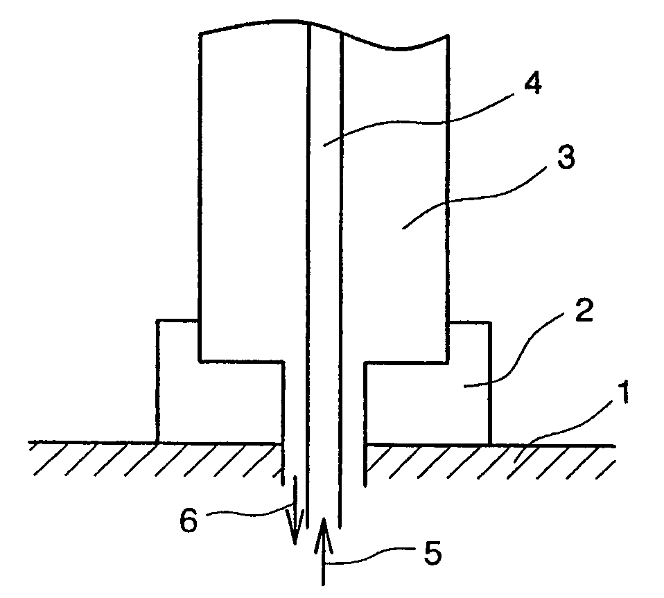
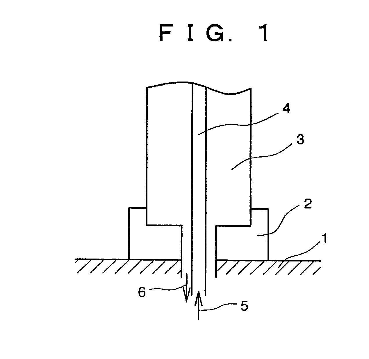
[0081]A hollow tube having an outer diameter of 9 mm and a height of 300 mm was prepared by subjecting, to a rounding work, a plate material of a lanthanum-added molybdenum alloy doped with lanthanum (La) of 0.1 mm thickness (trade name TEM Material: product by Allied Materials Co.). This was set in a gate form in a quartz glass bell jar (inner diameter 120 mm, height 500 mm), and was heated by passing electric current through. The method used for setting this in a gate form was as follows: namely, the upper end of each of the vertical tubes was cut into a V notch, and a horizontal pipe was mounted on top thereof. After the temperature of the core surface had reached 1180° C. as measured by an optical pyrometer, hydrogen gas after bubbling through a trichlorosilane liquid (temperature 25° C.) was supplied at 0.6 ml / minute, the hydrogen gas introduced directly into the reactor was supplied at 10.8 ml / minute, and hydrogen gas for reactor window use supplied to the inside surface of th...

example 2

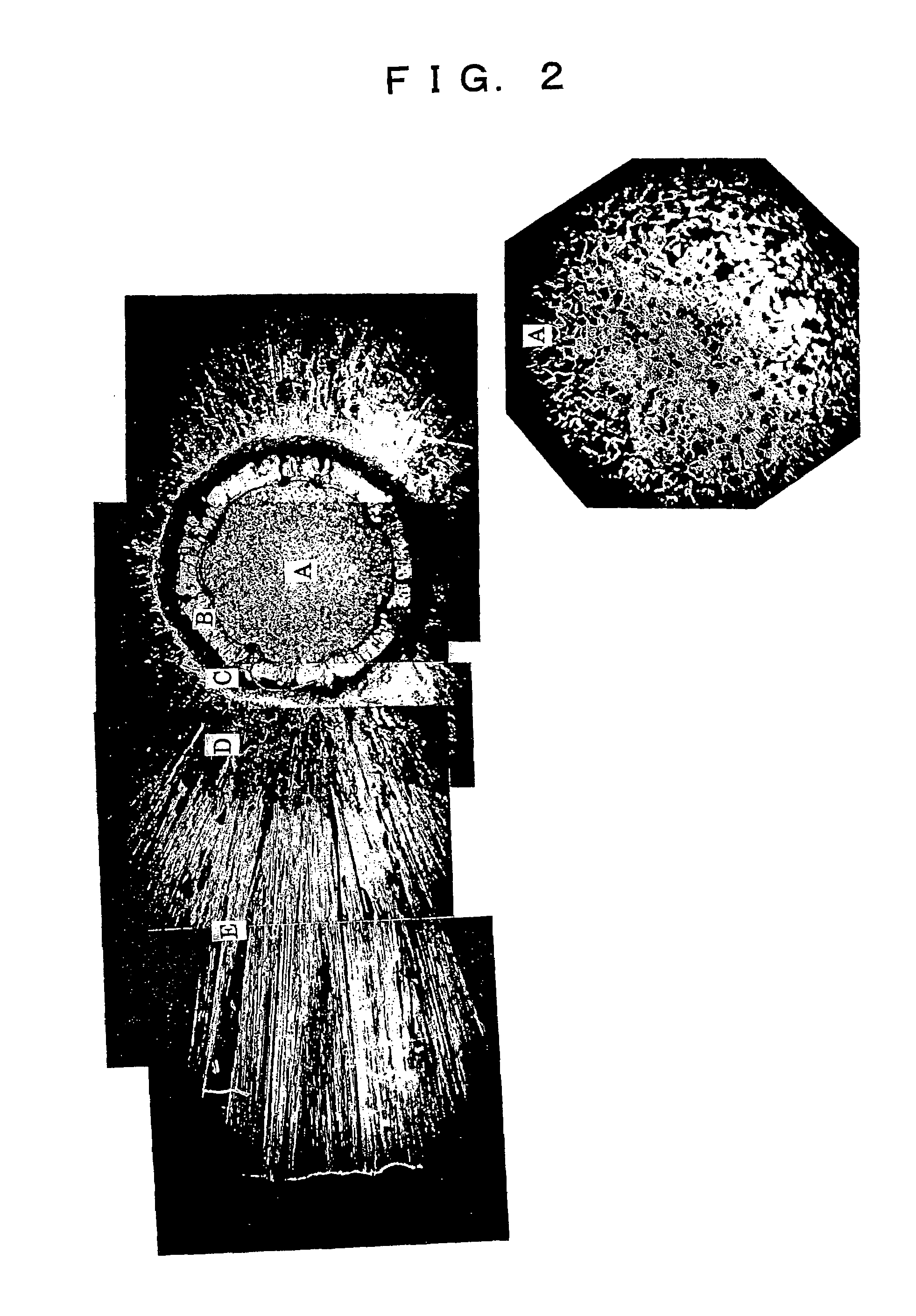
[0083]The reaction was performed in the same manner as in Example 1 using a TEM tube of the same dimensions as in Example 1. The TEM tube was heated for 10 hours at 1800° C. (in a hydrogen atmosphere) prior to the reaction, thus performing a treatment to prevent embrittlement. When the reaction was terminated after 8 hours lapse of time, and the diameter was measured, the diameter had grown to 16.2 mm. No heating means from outside was undertaken.

[0084]The block thus produced was subjected to the same treatment as in Example 1, and the conduction type, resistivity and lifetime of this block were measured. The results are shown in Table 1.

example 3

[0085]The reaction was performed in the same manner as in Example 1, except for the fact that the TEM tube used in Example 2 was reused. When the reaction was terminated after 8 hours lapse of time, and the diameter was measured, the diameter had grown to 16.1 mm. No heating means from outside was undertaken.

[0086]The block thus produced was subjected to the same treatment as Example 1, and the conduction type, resistivity and lifetime of this block were measured. The results are shown in Table 1. Furthermore, the amounts of Mo and La in the Si block following the reaction were determined. Both of these contents were not exceeding 1 ppb.


PUM

PropertyMeasurementUnit
temperatureaaaaaaaaaa
thicknessaaaaaaaaaa
diameteraaaaaaaaaa

Abstract

Provided is a method for the preparation of polycrystalline silicon in which, in conducting preparation of polycrystalline silicon by the Siemens method or by the monosilane method, no outer heating means is necessitated for the core member (seed rod), onto which polycrystalline silicon is deposited, from the initial stage of heating, the deposition rate is high and the core member seed rod can be used repeatedly.The method for deposition of high-purity polycrystalline silicon, at a high temperature, onto a white-heated seed rod in a closed reaction furnace by pyrolysis or hydrogen reduction of a starting silane gas supplied thereto, is characterized in that the seed rod is a member made from an alloy having a recrystallization temperature of 1200° C. or higher. It is preferable that the alloy member is of an alloy of Re—W, W—Ta, Zr—Nb, titanium-zirconium, or a carbon-added molybdenum (TZM) in the form of a wire member having a diameter of at least 0.5 mm, a plate member having a thickness of at least 1 mm or a prismatic member, or a tubular member having a diameter of at least 1 mm, wall thickness of at least 0.2 mm with an inner diameter not exceeding 5 mm, that the plate member, wire member, prismatic member or tubular member has a tapered form and further that the tubular member is a tapered duplex tube.

Description

TECHNOLOGICAL FIELD[0001]The present invention relates to a method for manufacturing high-purity polycrystalline silicon inexpensively and in large quantities, and in, particular, it is an object of the present invention to provide a solar cell silicon element with constancy.BACKGROUND ART[0002]The major currents of conventional methods for manufacturing high-purity polycrystalline silicon are the Siemens method and the monosilane method. These methods are methods in which a starting-material silane gas is supplied to the interior of a high-temperature reaction furnace from a nozzle installed in the bottom part of this sealed reaction furnace, and polycrystalline silicon is manufactured by the deposition or growth of silicon effected by the pyrolysis or hydrogen reduction of the starting-material gas on the surface of a solid silicon rod (silicon seed rod or core) disposed inside the furnace.[0003]The starting-material silane gas that is used is a chlorosilane expressed by the formu...

Claims


Application Information

Patent Timeline
Patent Type & Authority Patents(United States)
IPC IPC(8): C23C14/10B05D7/22C01B33/02C23C16/00C30B23/00C30B25/00C30B28/12C30B28/14H01L31/00C01B33/035H01L31/04H01L31/18
CPCC01B33/035H01L31/182Y02E10/546Y02P70/50
Inventor HONGU, TATSUHIKOKATO, YASUHIROHAGIMOTO, HIROSHI
Owner SHIN ETSU FILM
Why Eureka
Try Eureka