Method for the removal of surface oxides by electron attachment

a surface oxide and electron attachment technology, applied in the direction of metal-working equipment, non-electric welding equipment, solid-state devices, etc., can solve the problems of limiting the application of this approach, flammability of pure hydrogen, and drawbacks of the approach

Active Publication Date: 2013-06-04
AIR PROD & CHEM INC
View PDF21 Cites 4 Cited by
  • Summary
  • Abstract
  • Description
  • Claims
  • Application Information

AI Technical Summary

Problems solved by technology

One approach is fluxless soldering using pure hydrogen at a reflow temperature of 400 to 450° C. The major challenge of this approach is the flammable nature of the pure hydrogen, which largely limits the application of this approach.
However, this approach has its drawbacks.
Small voids may form in the solder bumps due to flux decomposition.
These voids may not only degrade the electrical and mechanical properties of the formed solder bonds but also destroy the co-planarity of the solder bumped wafer and affect the subsequent chip bonding process.
The decomposed flux volatiles can also contaminant the reflow furnace which can increase the maintenance cost.
In addition, flux residues are oftentimes left upon the wafer which can corrode metals and degrade the performance of the assembly.
However, post-cleaning adds an additional process step and increases the manufacturing processing time.
Further, the use of chlorofluorocarbons (CFCs) as cleaning agents is banned due to the potential damage to the earth's protective ozone layer.
Although no-clean fluxes have been developed by using a small amount of activators to reduce residues, there is a trade-off between the gain and loss in the amount of flux residues and the activity of the fluxes.
However, the melting or boiling points of the oxide and base metal can be similar and it may not be desirable to melt or vaporize the base metal.
Therefore, such laser processes are difficult to implement.
Lasers are typically expensive and inefficient to operate and require a direct line of sight to the oxide layer.
These factors limit the usefulness of laser techniques for most soldering applications.
Typical process temperatures exceed 350° C. However, this process can be slow and ineffective, even at elevated temperatures.
Vacuum operations require expensive equipment and must be performed as a slow, batch process rather than a faster, continuous process.
Also, plasmas are typically dispersed diffusely within the process chamber and are difficult to direct at a specific substrate area.
Therefore, the reactive species cannot be efficiently utilized in the process.
Plasmas can also cause damage to process chambers through a sputtering process, and can produce an accumulation of space charge on dielectric surfaces, leading to possible microcircuit damage.
Microwaves themselves can also cause microcircuit damage, and substrate temperature may be difficult to control during treatment.
Plasmas can also release potentially dangerous ultraviolet light.
Such processes also require expensive electrical equipment and consume considerable power, thereby reducing their overall cost effectiveness.
However, such hot cathode processes require vacuum conditions for optimum effectiveness and filament life.
Vacuum operations require expensive equipment, which must be incorporated into soldering conveyor belt systems, thereby reducing their overall cost effectiveness.
The resulting processes reduce oxides on the base metal to be soldered at temperatures near 150° C. However, such remote discharge chambers require significant equipment costs and are not easily retrofitted to existing soldering conveyor belt systems.
However, such dielectric shields can accumulate surface charge that may alter the electric field and inhibit precise process control.

Method used


Image

  • Method for the removal of surface oxides by electron attachment
  • Method for the removal of surface oxides by electron attachment
  • Method for the removal of surface oxides by electron attachment

Examples


example 1

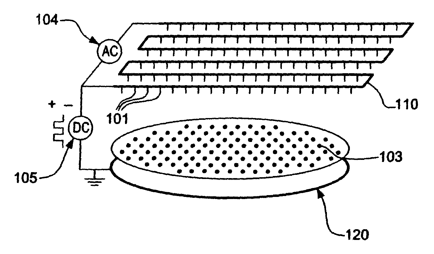
[0104]A first experiment was conducted by using a lab-scale furnace. The sample used was a fluxless tin-lead solder preform (melting point 183° C.) on a grounded copper plate (anode), which was loaded inside a furnace and heated up to 250° C. under a gas flow of 5% H2 in N2. When the sample temperature was at equilibrium, a DC voltage was applied between the negative electrode (cathode) and the grounded sample (anode) and gradually increased to about −2 kV with a current of 0.3 mA. The distance between the two electrodes was about 1 cm. The pressure was ambient, atmospheric pressure. It was found that the solder was indeed very well wetted on the copper surface. Without applying an electric voltage, a good wetting of a fluxless solder on a copper surface can never be achieved at such low temperature, even in pure H2, because the effective temperature for pure H2 to remove tin-oxides on a tin-based solder is above 350° C. Therefore, this result confirms that the electron-attachment m...

example 2

[0105]Several cathode materials were investigated for electron-attachment assisted hydrogen fluxless soldering by using the field emission mechanism using the same set-up as Example 1. The results of the investigation is provided in Table I.

[0106]As Table I illustrates, the best result was obtained by using a Ni / Cr cathode, which provided the highest fluxing efficiency and thus resulted in the shortest wetting time. It is believed that the Ni / Cr cathode generates a relatively larger quantity of electrons and has suitable energy level of the electrons compared to other cathode materials.

[0107]

TABLE IEffect of Cathode Material on Wetting Time at 250° C. and 20% H2Material of Cathode RodTime towith a Sharp Tip ( 1 / 16″ dia.)Complete WettingBrass1 min 55 secCopper1 min 44 secNickel Chromium39 secAluminum1 min 28 secStainless Steel1 minTungsten1 min 54 sec

example 3

[0108]The present example was conducted to investigate the effectiveness of the thermal-field emission method for generating electrons. A 3 mm diameter graphite rod, having a number of 1 mm long machined tips protruding from its surface, acted as the cathode and had a geometry similar to that depicted in FIG. 2i. Each of the protruding machined tips had a tip angle of 25 degrees. The graphite rod was heated up in a gas mixture of 5% H2 and 95% N2 to about 400 to 500° C. by resistive heating using an AC power source. A DC voltage source of 5 KV was applied between the graphite cathode and a copper plate that acted as an anode having a 1.5 cm gap therebetween. All the tips on the graphite rod were illuminated thereby indicating that electrons could uniformly be generated from the distributed tips on the graphite rod. Without heating of the graphite rod, there would be either no electron emission from the cathode, or arcing between one of the tips and the anode plate. This demonstrates...


PUM

PropertyMeasurementUnit
temperatureaaaaaaaaaa
distanceaaaaaaaaaa
voltageaaaaaaaaaa

Abstract

Described herein are a method and an apparatus for removing metal oxides and / or forming solder joints on at least a portion of a substrate surface within a target area. In one particular embodiment, the method and apparatus form a solder joint within a substrate comprising a layer having a plurality of solder bumps by providing one or more energizing electrodes and exposing at least a portion of the layer and solder bumps to the energizing electrode.

Description

CROSS-REFERENCE TO RELATED APPLICATIONS[0001]This application claims the benefit of U.S. Provisional Application No. 61 / 239,252, filed 2 Sep. 2009.BACKGROUND OF THE INVENTION[0002]Described herein are methods for removing metal oxides from the surface of a substrate, including an insulated substrate. Also described herein is an apparatus for removing metal oxides from the surface of a substrate.[0003]Wafer bumping is a process used to make thick metal bumps on the chip bond pads for inner lead bonding. The bumps are commonly made by depositing a solder on the pads and then reflowing (referred to herein as a first reflow) to conduct alloying and to change the shape of the solder bump from a mushroom-shape into a hemispherical-shape. The chip with the first-reflowed bumps is “flipped” to correspond to the footprint of the solder wettable terminals on the substrate and then subjected to a second reflow to form solder joints. These solder joints are referred to herein as inner lead bond...

Claims


Application Information

Patent Timeline
Patent Type & Authority Patents(United States)
IPC IPC(8): B23K31/02B08B13/00B08B7/00B23K1/20C23F1/08
CPCB23K1/008B23K35/262B23K35/38C23G5/00H01L21/02068H01L21/4864H01L21/67069H05K3/3489B23K1/206H01L2924/01322B23K2201/40C21D9/50H01L24/16H01L2224/16H01L2924/0102H01L2924/01077H01L2924/01078H01L2924/09701H01L2924/14H01L2924/3025H05K3/3457H05K2203/087H05K2203/105H01L2924/01087H01L2924/12042B23K2101/40H01L2924/00
Inventor DONG, CHUN CHRISTINEGHOSH, RANAJITARSLANIAN, GREGORY KHOSROV
Owner AIR PROD & CHEM INC
Why Eureka
Try Eureka