Apparatus and method for removal of surface oxides via fluxless technique involving electron attachment

a fluxless and electron attachment technology, applied in the direction of welding/cutting media/materials, welding apparatus, manufacturing tools, etc., can solve the problems of forming voids in solder joints, corrosion and electric shorts, and contaminating the reflow furnace, so as to improve the strength of the electric field

Active Publication Date: 2015-04-14
AIR PROD & CHEM INC
View PDF30 Cites 1 Cited by
  • Summary
  • Abstract
  • Description
  • Claims
  • Application Information

AI Technical Summary

Benefits of technology

[0020]The present invention solves some, if not all, of the problems of the art by providing a method and apparatus for removing metal oxides from at least one component and / or solder surface without requiring a flux, expensive vacuum equipment, and / or a flammable gas environment. In one aspect, there is provided an apparatus for removing metal oxides from the surface of a component comprising at least one selected from solder, metal, and combinations thereof through the emission of electrons in an ambient or non-vacuum pressure atmosphere by electron attachment comprising: a field emission apparatus comprising: a cathode having one or more protrusions and comprised of a conductive material wherein the material has a work function ranging from 2 to 5 eV; a dielectric material which surrounds at least a portion of the cathode; and an anode comprised of a conductive material which surrounds at least a portion of the dielectric material, wherein the cathode and anode are each connected to an electrical voltage source, and wherein the dielectric material between the cathode and anode is polarized wherein the dielectric material confines the electric field distribution and enhances the strength of the electric field near the one or more of the protrusions of the cathode and thereby emit electrons from the cathode. In this or other embodiments, at least a portion of the electrons are generated by one or more of the following processes: field emission, thermal-field emission, corona discharge, or combinations thereof.

Problems solved by technology

The fluxes are mostly evaporated into vapor phase during soldering; however, the flux volatiles may cause problems, such as forming voids in the solder joints and contaminating the reflow furnace.
After soldering, flux residues still remain on the circuit board that can cause corrosion and electric shorts.
The molten solder in the bath has a high tendency to be oxidized, forming solder dross.
Therefore the surface of the solder bath has to be frequently cleaned by mechanically removing the dross, which increases the operation cost and the consumption of the solder.
After soldering, flux residues remain on the circuit boards, which brings the same problems as described herein for reflow soldering.
However, this approach has its drawbacks.
Small voids may form in the solder bumps due to flux decomposition.
These voids may not only degrade the electrical and mechanical properties of the formed solder bonds but also destroy the co-planarity of the solder bumped wafer and affect the subsequent chip bonding process.
The decomposed flux volatiles can also contaminant the reflow furnace which can increase the maintenance cost.
In addition, flux residues are oftentimes left upon the wafer which can cause corrosion and degrade the performance of the assembly.
However, post-cleaning adds an additional process step and increases the manufacturing processing time.
Further, the use of chlorofluorocarbons (CFCs) as cleaning agents is banned due to the potential damage to the earth's protective ozone layer.
Although no-clean fluxes have been developed by using a small amount of activators to reduce residues, there is a trade-off between the gain and loss in the amount of flux residues and the activity of the fluxes.
One previously used hydrogen fluxless method for inner lead bonding has been to employ pure hydrogen for reflow of the solder bumped wafer at temperatures ranging from 400 to 450° C. However, the flammable nature of the pure hydrogen largely limits its application.
For soldering processes used in outer lead bonding, such as reflow soldering and wave soldering, the major limitation of using hydrogen to reduce surface oxides is the inefficient and slow reduction rate of metal oxides at the normal processing temperature ranges (<250° C.
This inefficiency of hydrogen is attributed to the lack of reactivity of the hydrogen molecule at low temperatures.
For example, the effective temperature range for pure H2 to reduce tin oxides on a tin-based solder is above 350° C. Such high temperatures may either damage or cause reliability problems to the packed electronic components.
However, the melting or boiling points of the oxide and base metal can be similar and it may not be desirable to melt or vaporize the base metal.
Therefore, such laser processes are difficult to implement.
Lasers are typically expensive and inefficient to operate and require a direct line of sight to the oxide layer.
These factors limit the usefulness of laser techniques for most soldering applications.
Typical process temperatures exceed 350° C. However, this process can be slow and ineffective, even at elevated temperatures.
Vacuum operations require expensive equipment and must be performed as a slow, batch process rather than a faster, continuous process.
Also, plasmas are typically dispersed diffusely within the process chamber and are difficult to direct at a specific area.
Therefore, the reactive species cannot be efficiently utilized in the process.
Plasmas can also cause damage to process chambers through a sputtering process, and can produce an accumulation of space charge on dielectric surfaces, leading to possible micro-circuit damage.
Microwaves themselves can also cause micro-circuit damage, and substrate or component temperature may be difficult to control during treatment.
Plasmas can also release potentially dangerous ultraviolet light.
Such processes also require expensive electrical equipment and consume considerable power, thereby reducing their overall cost effectiveness.
However, such hot cathode processes require vacuum conditions for optimum effectiveness and filament life.
Vacuum operations require expensive equipment, which must be incorporated into soldering conveyor belt systems, thereby reducing their overall cost effectiveness.
The resulting processes reduce oxides on the base metal to be soldered at temperatures near 150° C. However, such remote discharge chambers require significant equipment costs and are not easily retrofitted to existing soldering conveyor belt systems.
However, such dielectric shields can accumulate surface charge that may alter the electric field and inhibit precise process control.
Accordingly, there is a problem in the art in providing an economical and efficient process for removing metal oxides from at least one component and / or solder surface under relatively low temperatures to avoid damage to the electronic components.
There is a problem in the art in providing a process and apparatus for fluxless soldering under near ambient or atmospheric pressure conditions that avoids the expense of purchasing and maintaining vacuum equipment such as required, for example, in a plasma-based process and apparatus.
There is problem in providing a fluxless soldering process and apparatus for internal or non-exposed surfaces of a substrate.
Additionally, there is an additional problem in the art for providing a fluxless soldering process that does not involve one or more flammable gases.

Method used


Image

  • Apparatus and method for removal of surface oxides via fluxless technique involving electron attachment
  • Apparatus and method for removal of surface oxides via fluxless technique involving electron attachment
  • Apparatus and method for removal of surface oxides via fluxless technique involving electron attachment

Examples


example 1

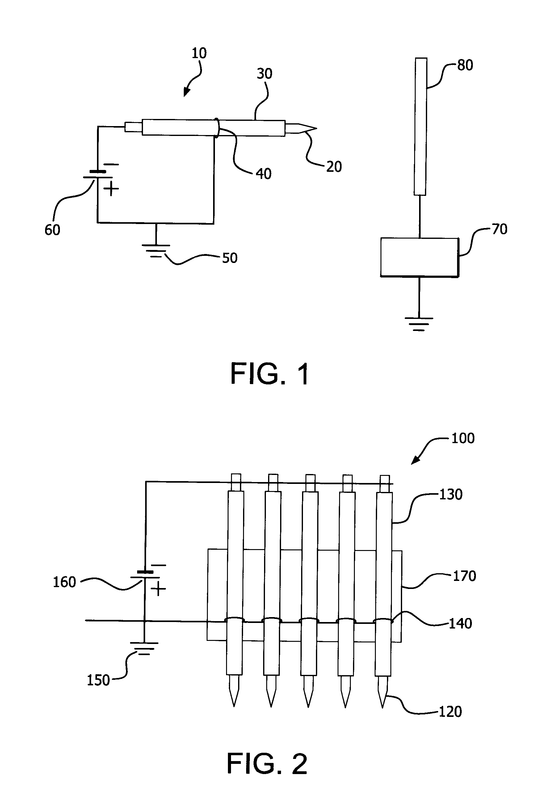
[0063]A field emission apparatus, such as that shown in FIG. 2 and containing five stainless steel cathode needles each tightly inserted into a dielectric material which comprised an alumina ceramic tube (0.46 mm inner diameter (I.D.) and 1.2 mm outer diameter (O.D.)) which was then mounted on a ceramic plate, was used in the present example. The distance between the cathode needles was 5 mm. The sharp tip of each cathode needle protruded about 1.0 mm out of the corresponding alumina ceramic tube. An anode metal wire was wound on each of the five tubes and electrically grounded. The wound anode wire was 10 mm away from the end of the tube toward the sharp tip side of the cathode needle. Such prepared structure was located in a quartz tube furnace purged with 4 vol % H2 in N2 at room temperature. When a pulsed (10 KV) negative voltage potential applied on the five needles was increased to −3.7 KV, all the five needle tips started to emit electrons. When electron emission starts on a ...

example 2

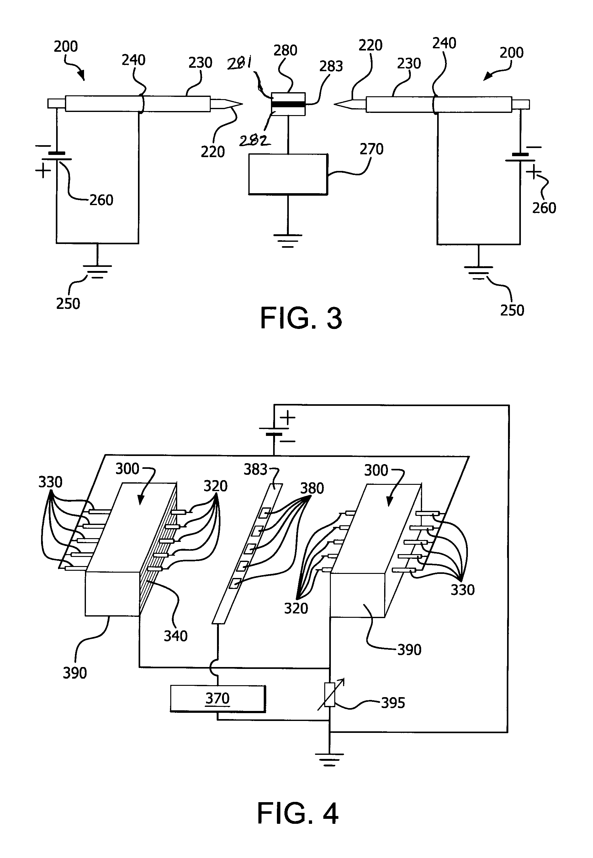
[0064]A field emission apparatus structure, which contains two stainless steel cathode needles each inserted with a ceramic (alumina) tube or dielectric material and mounted on both sides of a die attachment sample placed on a copper plate such as the configuration shown in FIG. 3 was tested. The die attachment sample was electrically conductive and grounded. The distance between each needle tip and the sample edge was 5.5 mm. The sharp tip of each cathode needle extended 1.0 mm out of the corresponding dielectric tube. An anode metal wire was wound upon each of the two dielectric materials or tubes and electrically grounded. The wound anode wire was 10 mm away from the end of the tube toward the sharp tip side. Such prepared structure was located in a quartz tube furnace purged with 4 vol % H2 in N2 at room temperature. When a pulsed (10 KV) negative voltage potential applied on the two needles was increased to −1.9 KV, the two needle tips lit up in a blue color, indicating electro...

example 3

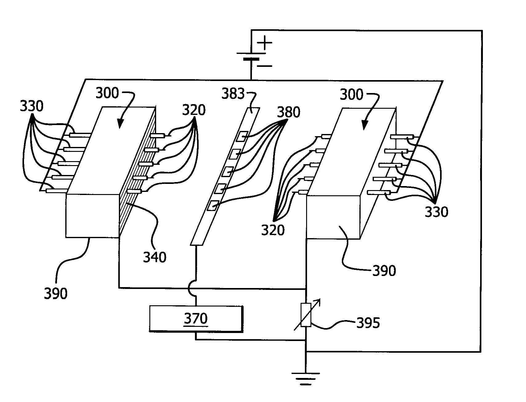
[0065]The same field emission apparatus structure and the sample arrangement described in Example 2 and FIG. 3 was tested again in a quartz tube furnace purged with 15 vol % H2 in N2. The die attachment sample 280 contained a fluxless gold / tin solder preform (m.p. 280° C.) 283 sandwiched by a gold / nickel coated ceramic 281 and a gold / nickel coated copper 282, which were used to simulate die attachment device. The three pieces of the die attachment sample each had the same size: 3 mm×6 mm. To demonstrate the feasibility of electron attachment (EA) activated H2 in N2 for fluxless die attachment, a pulsed (10 KV) negative voltage potential was applied on the two needles at room temperature. When the applied voltage was increased to −1.8 KV, the two needle tips lit up in a blue color, indicating electron emission. The current received on the sample was −0.45 mA. The sample was then heated up to 290° C. in a ramp time of two minutes and soaked at 290° C. for one minute before cooling dow...


PUM

PropertyMeasurementUnit
work functionaaaaaaaaaa
electrical potentialaaaaaaaaaa
pore sizeaaaaaaaaaa

Abstract

Described herein is a method and apparatus for removing metal oxides on a surface of a component via electron attachment. In one embodiment, there is provided a field emission apparatus, wherein the electrons attach to at least a portion of the reducing gas to form a negatively charged atomic ions which removes metal oxides comprising: a cathode comprising an electrically conductive and comprising at least one or more protrusions having a high surface curvature, wherein the cathode is surrounded by a dielectric material which is then surrounded by an electrically conductive anode wherein the cathode and anode are each connected to an electrical voltage source, and the dielectric material between the cathode and anode is polarized to provide an electric field at one or more protrusions and thereby electrons from the cathode.

Description

CROSS-REFERENCE TO RELATED APPLICATIONS[0001]This application claims the benefit of U.S. Provisional Application Nos. 61 / 441,053, filed 9 Feb. 2011 and 61 / 563,112 filed 23 Nov. 2011.BACKGROUND OF THE INVENTION[0002]The present invention relates generally to fluxless processes for removing surface oxides. More specifically, the invention relates to an apparatus and method comprising same for fluxless reflow and soldering involving electron attachment and field emission at ambient (e.g., non vacuum) pressure.[0003]Reflow and soldering are important processing steps in the assembly of electronic components for making solder joints. The term “reflow” as used herein refers to a process for making a previously applied solder on a substrate melt and flow upon application of an energy source such as, for example, thermal energy. The term “soldering” as used herein refers to a process that allows a melted solder to join at least two metallic substrates. A variety of different reflow and sold...

Claims


Application Information

Patent Timeline
Patent Type & Authority Patents(United States)
IPC IPC(8): H01J7/24B01J19/08B23K1/20B23K35/38C23G5/024
CPCB23K1/203B01J19/088B23K35/38C23G5/024H01L2924/0002H01L2924/00H01L21/02
Inventor DONG, CHUN CHRISTINESIMINSKI, RUSSELL A.
Owner AIR PROD & CHEM INC
Why Eureka
Try Eureka