Manufacturing method of group III nitride semiconductor

a manufacturing method and semiconductor technology, applied in the direction of polycrystalline material growth, chemically reactive gas growth, crystal growth process, etc., can solve the problems of iii nitride semiconductor, large number of threading dislocations, deterioration of surface flatness, etc., to control the crystalline quality and surface flatness of the second layer, and simplify the manufacturing process

Active Publication Date: 2013-06-18
TOYODA GOSEI CO LTD
View PDF13 Cites 3 Cited by
  • Summary
  • Abstract
  • Description
  • Claims
  • Application Information

AI Technical Summary

Benefits of technology

[0015]In the exemplary embodiments of the present invention, the surfactant is an impurity which induces a two dimensional growth by restricting the vertical growth (growth perpendicular to the main surface of the substrate) and promoting the lateral growth (growth parallel to the main surface of the substrate). The anti-surfactant is an impurity which induces a three dimensional growth by restricting the lateral growth and promoting the vertical growth. The impurities acting as a surfactant for the group III nitride semiconductors are p-type impurities such as Mg. The impurities acting as an anti-surfactant for the group III nitride semiconductors are n-type impurities such as Si. The actions of these impurities as a surfactant or an anti-surfactant are generally enhanced as the concentration of the impurities increase.
[0038]According to the sixteenth aspect of the exemplary embodiment of the present invention, it is possible to control the crystalline quality and the surface flatness of the second layer by controlling dopant only if the first layer and the second layer are grown under the same condition. Therefore, the manufacturing process can be simplified.

Problems solved by technology

This lattice constant mismatch causes large number of threading dislocations in the group III nitride semiconductors.
Thus grown group III nitride semiconductor, however, has deteriorated flatness of the surface because of pits formed thereon and is not suitable for device purposes.
If the concentration of Mg or Si is larger than these ranges, the crystalline quality is deteriorated.
In the exemplary embodiments, non-dope does not eliminate the possibility of impurity doping which act as neither a surfactant nor an anti-surfactant.

Method used


Image

  • Manufacturing method of group III nitride semiconductor
  • Manufacturing method of group III nitride semiconductor
  • Manufacturing method of group III nitride semiconductor

Examples


first exemplary embodiment

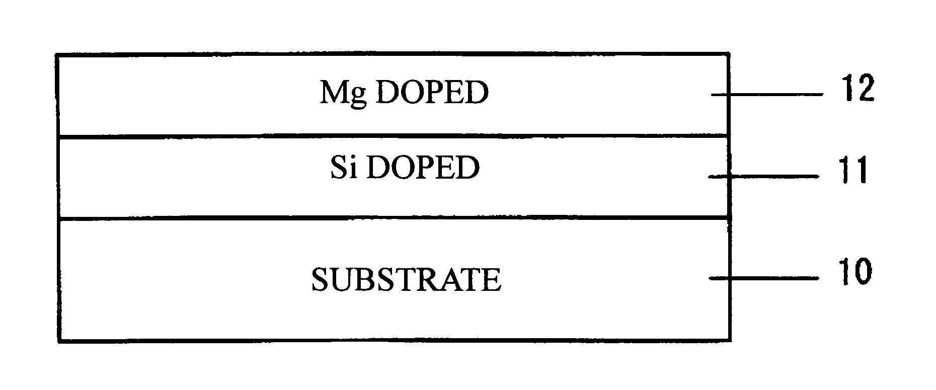
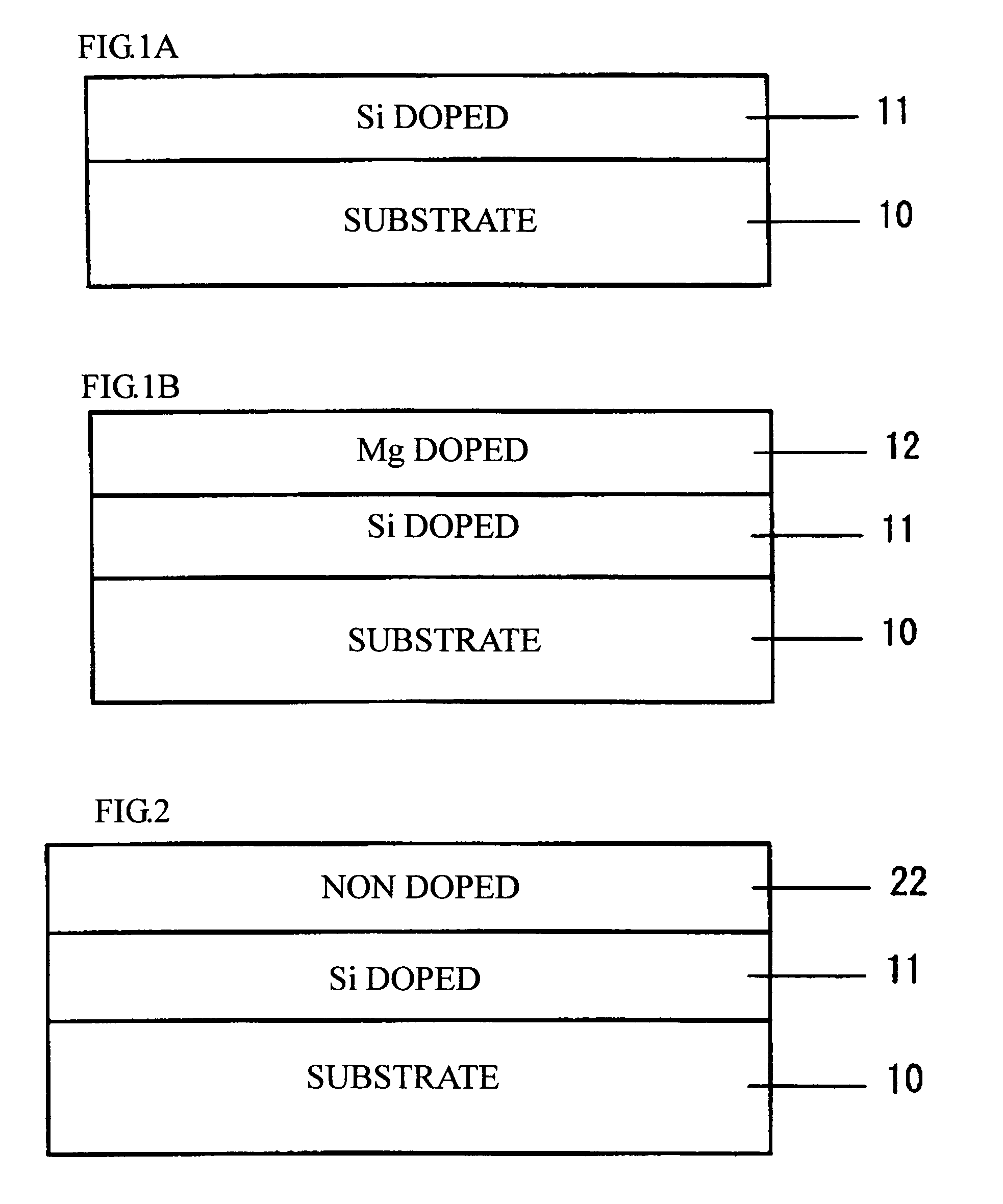
[0047]A sample according to the first exemplary embodiment was manufactured by the manufacturing method described below. At first, a sapphire substrate 10, whose surface was flat and was not worked, was prepared. The sapphire substrate 10 was annealed in hydrogen atmosphere so as to remove surface adsorbates. Then, a Si doped GaN layer (corresponding to the first layer) 11 was formed by MOCVD on the surface of the sapphire substrate 10 via buffer layer of AIN (not shown) (FIG. 1A). The Si concentration in the Si doped GaN layer 11 was set within the range from 1×10¹⁸ to 1×10²⁰ / cm3 and the thickness of the Si doped GaN layer 11 was 1 μm. For the MOCVD process, the carrier gas was hydrogen gas and nitrogen gas, the nitrogen source was ammonia, the gallium source was TMG (trimethylgallium), and the dopant gas was silane (SiH4). The growth conditions such as the growth temperature and pressure were usually adopted conditions for the crystal growth of the group III nitride semiconductors...

second exemplary embodiment

[0059]A sample of the second exemplary embodiment is shown in FIG. 2. The sample of the second exemplary embodiment was same as the samples according to the first exemplary embodiment except for that the sample has a non-doped GaN layer 22 instead of the Mg doped GaN layer 12 in the first exemplary embodiment. The growth conditions such as the growth temperature and pressure for the non-doped GaN layer 22 was same as those of the first exemplary embodiment. In the crystal growth of the non-doped GaN layer 22, the three dimensional growth is relatively dominant but the tendency of the three dimensional growth is less than that of the Si doped GaN layer 11. Therefore, it is possible to gradually change the crystal growth mode from three dimensional growth to the weak three dimensional growth by stacking the Si doped GaN layer 11 ad the non-doped GaN layer 22 in this order. As a result, the number of the threading dislocation can be reduced and the high surface flatness can be achieved...

third exemplary embodiment

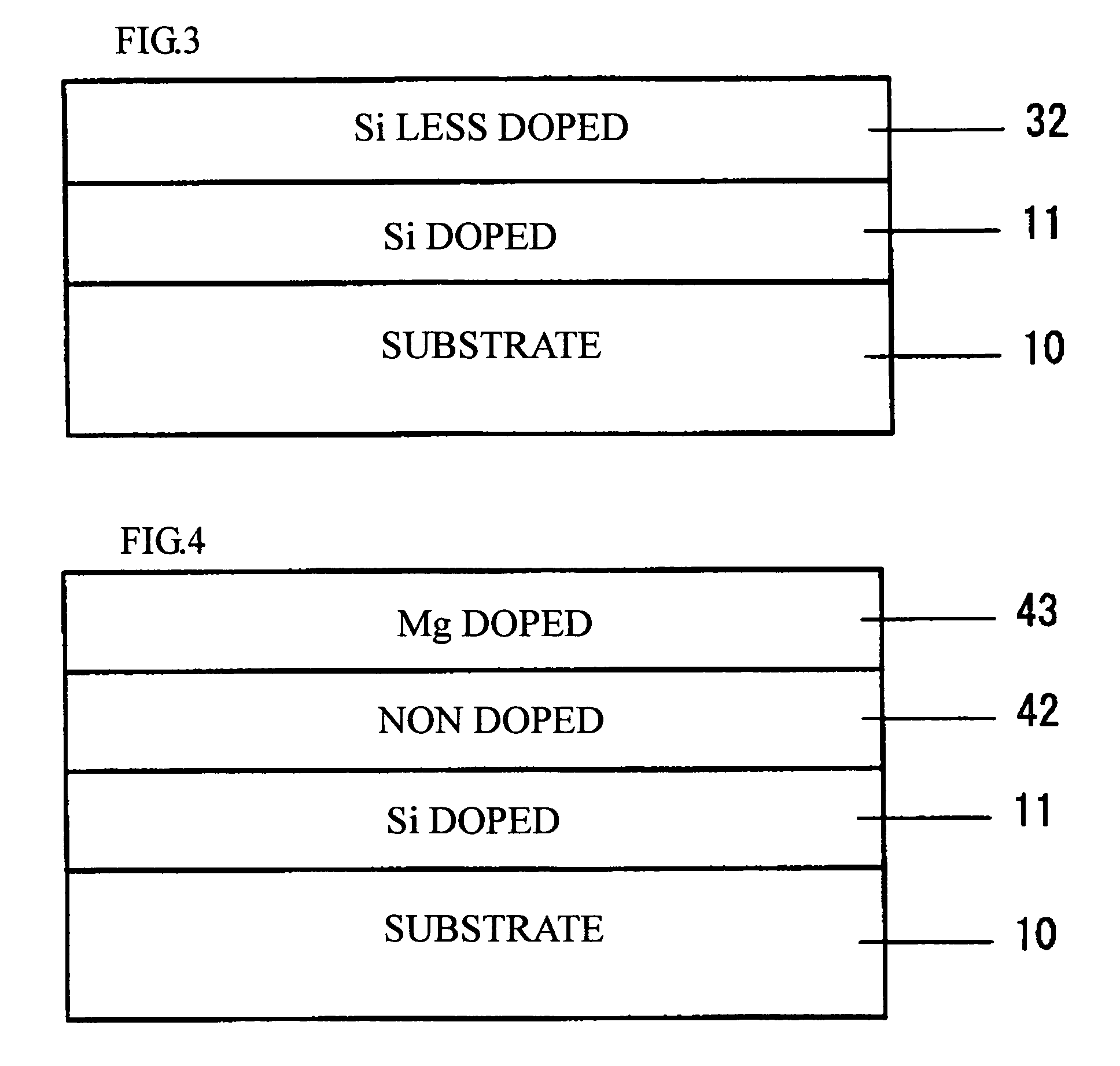
[0062]A sample of the third exemplary embodiment is shown in FIG. 3. The sample of the third exemplary embodiment is same as the exemplary embodiment 1 except for that the sample has a Si less doped GaN layer 32 instead of the Si doped GaN layer 12 in the first exemplary embodiment. The Si concentration in the Si less doped GaN layer 32 is lower than that in the Si doped GaN layer 11. The Si less doped GaN layer 32 less favors the three dimensional growth as compared to the Si doped GaN layer 11. Therefore, it is possible to gradually change the growth mode from the three dimensional growth to the weak three dimensional growth by stacking the Si doped GaN layer 11 and the Si less doped GaN layer 32 in this order. As a result, it is possible to reduce the number of the threading dislocation and improve the surface flatness.

[0063]The crystalline quality of the Si less doped GaN layer 32 in the c-plane of a sample 3A according to the third exemplary embodiment was evaluated. In the sam...


PUM

PropertyMeasurementUnit
thicknessaaaaaaaaaa
surface flatnessaaaaaaaaaa
thicknessaaaaaaaaaa

Abstract

A manufacturing method of a group III nitride semiconductor comprising: preparing a substrate including a buffer layer; forming a first layer on the buffer layer from a group III nitride semiconductor by MOCVD while doping an anti-surfactant, wherein a thickness of the first layer is equal to or thinner than 2 μm; forming a second layer on the first layer from a group III nitride semiconductor by MOCVD while doping at least one of surfactant and an anti-surfactant; and controlling a crystalline quality and a surface flatness of the second layer by adjusting an amount of the anti-surfactant and the surfactant doped during the formation of the second layer.

Description

CROSS REFERENCE TO RELATED APPLICATIONS[0001]This application claims priority from Japanese Patent Application No. 2009-071868 filed on Mar. 24, 2009, and the subject matter of which is incorporated herein by reference.TECHNICAL FIELD[0002]The present invention relates to a manufacturing method of high quality group III nitride semiconductors with few threading dislocations.BRIEF DESCRIPTION OF RELATED ART[0003]Group III nitride semiconductors such as gallium nitride (GaN) are used as a material for a light emitting diode (LED) and a semiconductor laser element. Recently, the group III nitride semiconductors draw attention as a material for high frequency devices and power devices.[0004]For the purpose of a crystal growth of the group III nitride semiconductors, hetero-type substrates such as a sapphire substrate are used. Such hetero-type substrates have a lattice constant different from that of the group III nitride semiconductors. This lattice constant mismatch causes large numbe...

Claims


Application Information

Patent Timeline
Patent Type & Authority Patents(United States)
IPC IPC(8): H01L33/00
CPCH01L21/0242H01L21/02458H01L21/02502H01L21/02505H01L21/0254H01L21/02573H01L21/02609
Inventor OKUNO, KOJI
Owner TOYODA GOSEI CO LTD
Why Eureka
Try Eureka