Underlayer composition and process thereof

a composition and layer technology, applied in the field of underlayer composition and process thereof, can solve the problems of back reflectivity, thin film interference effect and reflective notching, and change in critical line width dimensions

Active Publication Date: 2013-10-29
MERCK PATENT GMBH
View PDF24 Cites 16 Cited by
  • Summary
  • Abstract
  • Description
  • Claims
  • Application Information

AI Technical Summary

Benefits of technology

[0005]Absorbing antireflective coatings and underlayers in photolithography are used to diminish problems that result from back reflection of light from highly reflective substrates. Two major disadvantages of back reflectivity are thin film interference effects and reflective notching. Thin film interference, or standing waves, result in changes in critical line width dimensions caused by variations in the total light intensity in the photoresist film as the thickness of the photoresist changes or interference of reflected and incident exposure radiation can cause standing wave effects that distort the uniformity of the radiation through the thickness. Reflective notching becomes severe as the photoresist is patterned over reflective substrates containing topographical features, which scatter light through the photoresist film, leading to line width variations, and in the extreme case, forming regions with complete photoresist loss. An antireflective coating film coated beneath a photoresist and above a reflective substrate provides significant improvement in lithographic performance of the photoresist. Typically, the bottom antireflective coating is applied on the substrate and then a layer of photoresist is applied on top of the antireflective coating. The antireflective coating is cured to prevent intermixing between the antireflective coating and the photoresist. The photoresist is exposed imagewise and developed. The antireflective coating in the exposed area is then typically dry etched using various etching gases, and the photoresist pattern is thus transferred to the substrate.
[0006]Underlayers containing high amount of refractory elements, such as titanium or silicon, can also be used as hard masks after being patterned by an overlying photoresist. Such hard masks are useful when the overlying photoresist is very thin and is not capable of providing high enough dry etch resistance required for transferring the image into the underlying semiconductor substrate. In such circumstances it is useful to coat the photoresist on a coating composed of an inorganic material called a hard mask whose etch resistance is high enough to transfer any patterns created over it into the underlying semiconductor substrate. This is made possible because the organic resist is different than the underlying hard mask and it is possible to find an etch gas mixture which will allow the transfer of the image in the resist into the underlying hard mask. This patterned hard mask can then be used with appropriate etch conditions and gas mixtures to transfer the image from the hard mask into the semiconductor substrate, a task which the resist by itself with a single etch process could not have accomplished. Multiple antireflective layers and underlayers are being used in new lithographic techniques. In cases where the photoresist does not provide sufficient dry etch resistance, underlayers and / or antireflective coatings for the photoresist that act as a hard mask and are highly etch resistant during substrate etching are preferred, and one approach has been to incorporate silicon or titanium into a layer beneath the organic photoresist layer. Additionally, another high carbon content antireflective or mask layer is placed beneath the silicon or titanium antireflective layer, such a trilayer of high carbon film / hardmask film / photoresist is used to improve the lithographic performance of the imaging process. Conventional hard masks can be applied by chemical vapor deposition, sputtering. However, the relative simplicity of spin coating versus the aforementioned conventional approaches makes the development of a new spin-on a hard mask with high concentration of titanium in the film very desirable.
[0007]The present invention relates to novel titanium compositions and processes. The novel organic titanate based underlayers have sufficient titanium in the film, depending on the amount of titanium compound present in the composition and the curing process used. The underlayer coating has good resistance to both casting solvent and aqueous alkaline developer over a wide range of both titanium concentration and also optical indices. The coating and crosslinking quality of the underlayer coating is at least comparable to conventional nonmetallic organic bottom antireflective coatings. The novel underlayer compositions also have good stability with long term storage.
[0008]The present invention relates to a spin-on coating material useful for generating titanium containing underlayers. The composition has good long term shelf life stability. The film of the novel composition has excellent dry etch resistance and can be used as a hard mask to replace silicon underlayers in many processes, such as trilayer imaging processes. The underlayer coating is capable of absorbing deep ultraviolet radiation and can be used as spin-on inorganic or hybrid antireflective coating to control substrate reflectivity when exposed to deep ultraviolet radiation. The novel composition can also be used as an underlayer in extreme ultraviolet (EUV) lithography to significantly improve photosensitivity, which helps to improve overall EUV photoresist performance. Additionally, the novel composition is capable of forming spin coatable and crosslinked titanium coatings which may be used for many other applications.SUMMARY OF THE INVENTION

Problems solved by technology

Two major disadvantages of back reflectivity are thin film interference effects and reflective notching.
Thin film interference, or standing waves, result in changes in critical line width dimensions caused by variations in the total light intensity in the photoresist film as the thickness of the photoresist changes or interference of reflected and incident exposure radiation can cause standing wave effects that distort the uniformity of the radiation through the thickness.
Such hard masks are useful when the overlying photoresist is very thin and is not capable of providing high enough dry etch resistance required for transferring the image into the underlying semiconductor substrate.

Method used


Image

  • Underlayer composition and process thereof
  • Underlayer composition and process thereof
  • Underlayer composition and process thereof

Examples


examples

[0046]The refractive index (n) and the absorption (k) values of the antireflective coating in the Examples below were measured on a J. A. Woollam VASE32 ellipsometer.

[0047]The molecular weight of the polymers was measured on a Gel Permeation Chromatograph.

synthesis example

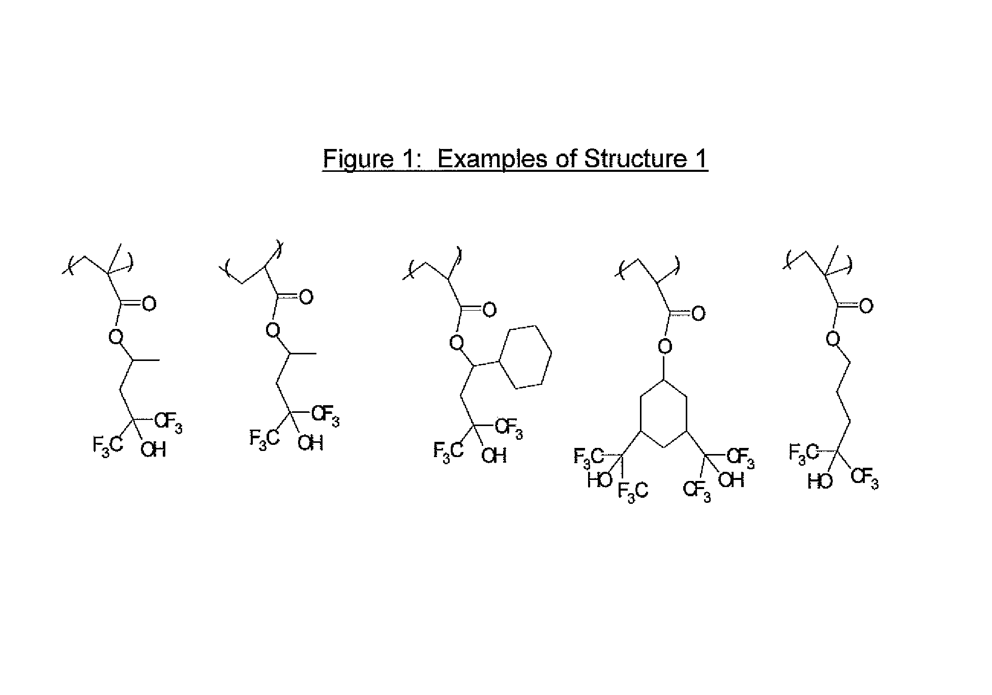
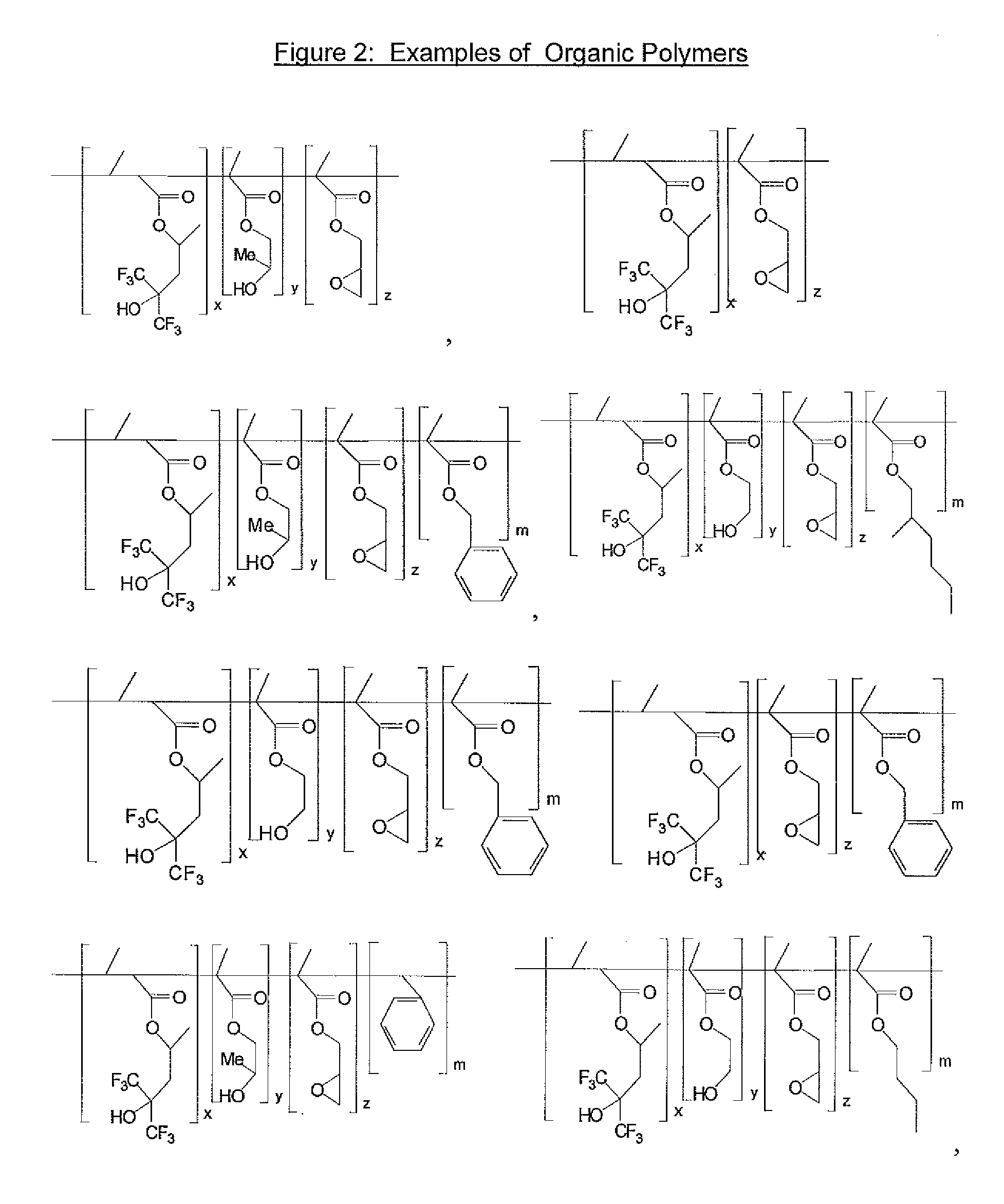
[0048]12.9 g of isopropyl hexafluoroisopropanol methacrylate (MA-BTHB-OH), 7.7 g of benzyl methacrylate, 6.8 g of 2-hydroxyethyl methacrylate and 8.5 g of glycidyl methacrylate, were mixed with 160 g of propyleneglycol monomethyl ether (PGME) solvent. The polymerization reaction took place in the presence of 1.5 g of azobisisobutyronitrile (AIBN) at 75° C. under nitrogen for 6 hours. After cooling down to room temperature, the reaction mixture was precipitated in deionized (DI) water. The white polymer solid was washed and dried under vacuum at 45° C. with a yield of 35.5 g (99%). The weight average molecular weight measured by GPC (Mw) was 18,000.

synthesis example 2

[0049]9.7 g of MA-BTHB-OH, 5.8 g of benzyl methacrylate, 5.1 g of 2-hydroxyethyl methacrylate and 6.4 g of glycidyl methacrylate, were mixed with in 120 g of tetrahydrofuran (THF) solvent. The polymerization reaction took place in the presence of 1.0 g of AIBN at 75° C. under nitrogen for 20 hrs. After cooling down to room temperature, the reaction mixture was precipitated in DI water. The white polymer solid was washed and dried under vacuum at 45° C. with a yield of 26.5 g (99%) The Mw of polymer measured by GPC was 19,000.


PUM

PropertyMeasurementUnit
refractive indexaaaaaaaaaa

Abstract

The present invention relates to an underlayer composition comprising a polymer, an organic titanate compound and optionally a thermal acid generator, where the polymer comprises at least one fluoroalcohol group and at least one epoxy group. The invention also relates to a process for using this underlayer material as an antireflective coating composition and / or a hard mask for pattern transfer.

Description

[0001]The present invention relates to compositions of a spin-on metal containing underlayers for photolithographic processes, and a process for imaging using such layers.[0002]Photoresist compositions are used in microlithography processes for making miniaturized electronic components such as in the fabrication of computer chips and integrated circuits. Generally, in these processes, a thin coating of film of a photoresist composition is first applied to a substrate material, such as silicon based wafers used for making integrated circuits. The coated substrate is then baked to evaporate any solvent in the photoresist composition and to fix the coating onto the substrate. The baked coated surface of the substrate is next subjected to an image-wise exposure to radiation.[0003]This radiation exposure causes a chemical transformation in the exposed areas of the coated surface. Visible light, ultraviolet (UV) light, electron beam and X-ray radiant energy are radiation types commonly us...

Claims


Application Information

Patent Timeline
Patent Type & Authority Patents(United States)
IPC IPC(8): G03F7/20G03F7/00C08K5/04C08K5/00H01L51/00
CPCC08K5/0091C08L33/16C08L101/06G03F7/091G03F7/094C08L33/04C08L37/00C08K5/56G03F7/00H10K99/00
Inventor YAO, HUIRONGLIN, GUANYANGBOGUSZ, ZACHARYLU, PINGHUNGKIM, WOOKYUNEISSER, MARK
Owner MERCK PATENT GMBH
Why Eureka
Try Eureka