

Method of fabricating free-form, high-aspect ratio components for high-current, high-speed microelectronics
a microelectronic and high-speed technology, applied in the field of three-dimensional microelectronic structures, can solve the problems of non-intuitive, difficult to create 3-d electronic components and devices, and more complex structures may be created
- Summary
- Abstract
- Description
- Claims
- Application Information
AI Technical Summary
Benefits of technology
Problems solved by technology
Method used
Image

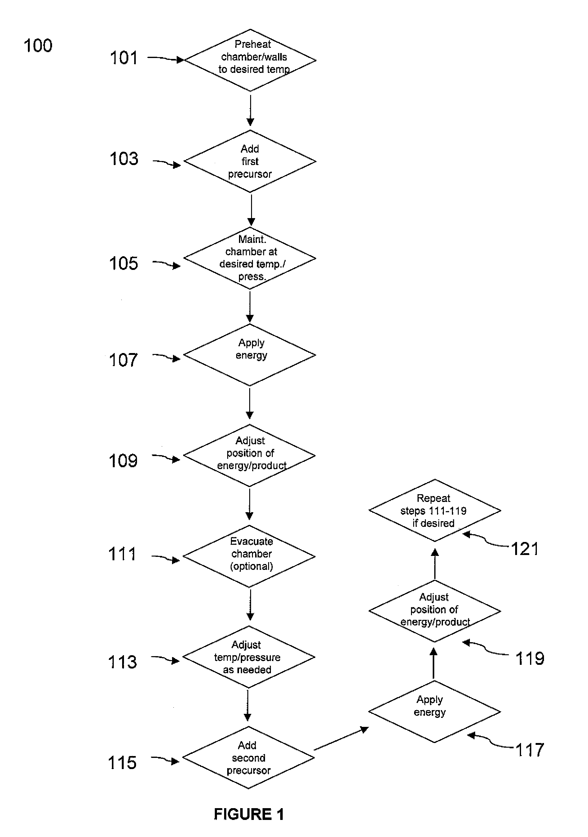
Examples
example 1
Tungsten Fibers
[0067]Several dozen pure tungsten fibers were grown using WF6+H2 or WCl6+H2 gas mixtures. WF6+H2 proved to be the superior precursor system for both growth rates and lack of deposit impurities. Even at hyperbaric pressures, the kinetics of WCl6+H2 deposition was very slow. Using WF6+H2, very rapid steady-state growth rates were obtained, ranging from 3-160 μm / s. Typical gas mixtures were 3:1 H2 to WF6, and a cw Ar+ laser was used at laser powers from 400 mW to 12 W. The purity of the deposit was examined by energy dispersive X-ray spectroscopy (EDS) and Auger spectroscopy. Essentially no trace of fluorine was detected in the deposits, and only a thin native oxide was present, due to exposure to air prior to characterization. The microstructures of the fibers varied greatly, depending on the precursor pressures and laser powers employed. At WF6 partial pressures of 350 mbar and laser powers of 800-900 mW, the fine tungsten fibers grew as highly-oriented single-crystals...
example 2
[0068]A three-dimensional Shottky diode was fabricated as follows. An indium-doped silicon fiber was grown using as precursors materials for indium trimethylindium ((CH3)3In) and cyclopentadienylindium (C5H5In) and as precursor materials for silicon silane (SiH4) and disilane (Si2H6). To achieve sufficient conductivity of the silicon single-crystals, the concentration of indium precursors in the gas phase may be less than 1000 ppm. The chamber pressure ranged from 600-1200 torr, and a cw Nd:YAG laser was used at laser powers from 200 mW to 3 W. An electrode also could be used to impart comparable energy, as would be understood by one of skill in the art.
[0069]The quantity of indium was slowly decreased, while adding very small quantities of boron (<1 torr) by means of a boron precursor. Suitable boron precursors include among others diborane, trimethylboron, triethylboron, triphenylboron, and decaborane. The slow addition of boron creates a boron-doped section in the s...
example 3
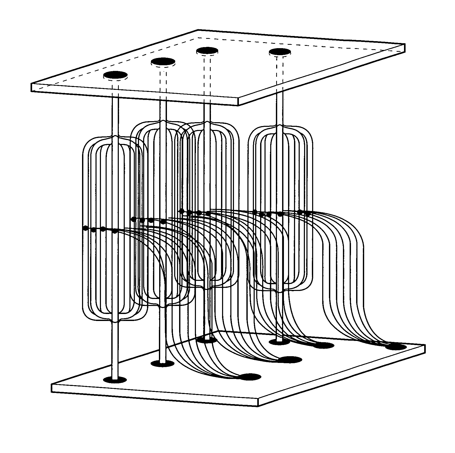
[0073]A hybrid three-dimensional micromechanical spring assembly, electrical coil, and electrodes were fabricated as follows: A supporting fiber was grown of carbon from ethylene. A soft mechanical spring was created of hydrogenated diamond-like carbon from ethylene and hydrogen. The growth rates were 15-20 microns per second, and the laser power was approximately 300-400 mW. Probes and coils were fabricated of carbon and tipped / coated with proprietary metals. This assembly was only 2-3 mm long, and functioned as a rudimentary accelerometer that responds to frequencies down to about 25 Hz.
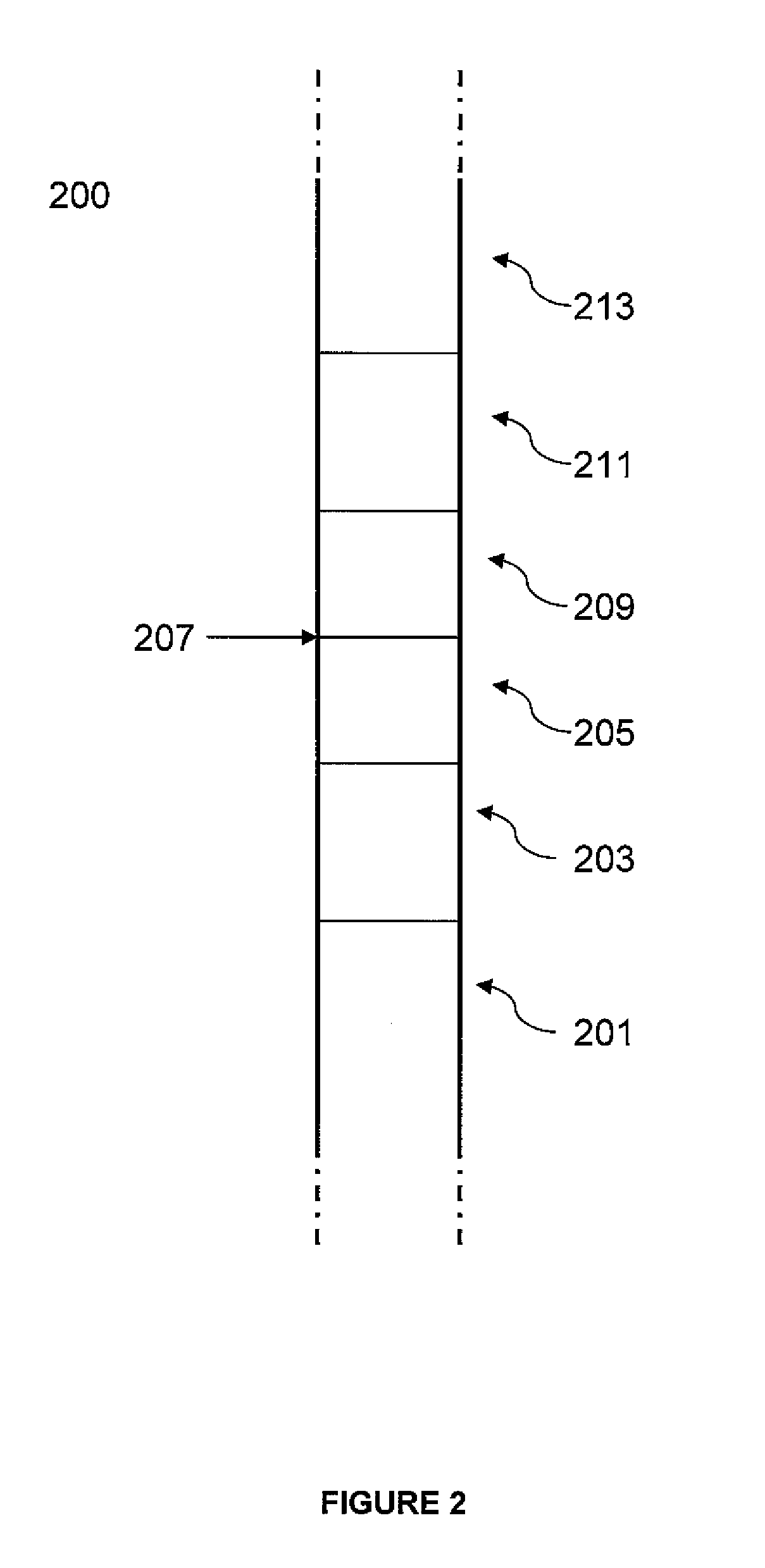
[0074]In all embodiments of the present invention, all percentages are by weight of the total composition, unless specifically stated otherwise. All ratios are weight ratios, unless specifically stated otherwise. All ranges are inclusive and combinable. The number of significant digits conveys neither a limitation on the indicated amounts nor on the accuracy of the measurements. All numerical amoun...
PUM
| Property | Measurement | Unit |
|---|---|---|
| pressure | aaaaa | aaaaa |
| pressure | aaaaa | aaaaa |
| diameter | aaaaa | aaaaa |
Abstract
Description
Claims
Application Information