Method for manufacturing group III nitride semiconductor, method for manufacturing group III nitride semiconductor light-emitting device, group III nitride semiconductor light-emitting device, and lamp
a technology of nitride semiconductor and manufacturing group, which is applied in the direction of crystal growth process, polycrystalline material growth, electric/magnetic/electromagnetic heating, etc., can solve the problems of lowering the production yield, extremely reducing the formation rate, and not commercially available iii nitride semiconductor, etc., to achieve the effect of enhancing the initial dislocation loop, reducing the dislocation density of a crystal, and increasing the film formation rate of crystal
- Summary
- Abstract
- Description
- Claims
- Application Information
AI Technical Summary
Benefits of technology
Problems solved by technology
Method used
Image
Examples
example 1
[0182]In Example 1, according to the following procedure, the buffer layer 12 was formed on the substrate 11 by using the reactive sputtering method, and then the GaN layer (ground layer 14a) was formed thereon by using the reactive sputtering method.
[Formation of Buffer Layer]
[0183]At first, the substrate 11 made of sapphire having a (0001) c plane of a diameter of 2 inches, the surface of which had been mirror finished, was washed with hydrofluoric acid or organic solvent, and was then introduced into a chamber of a sputtering apparatus. Here, as the sputtering apparatus, there was employed an apparatus having a high frequency-type power supply, and a mechanism capable of moving a position influenced by the magnetic field, through rotation of a magnet within a target.
[0184]The substrate 11 was heated to 500° C. in the chamber of the sputtering apparatus, into which a nitrogen gas was introduced at a flow rate of 15 sccm. Then, while keeping the pressure in the chamber at 1.0 Pa an...
example 2
[0197]In Example 2, according to the following procedure, the buffer layer 12 was formed on the substrate 11 using the sputtering apparatus 40 shown in FIG. 5, and then the ground layer 14a made of GaN was formed thereon.
[0198]In present Example, firstly, the buffer layer 12 made of AlN having a single-crystalline structure was formed on the c plane of the substrate 11 made of sapphire using the sputtering apparatus 40 according to the same procedure as in Example 1. The ground layer 14a of the n-type semiconductor layer 14 made of the undoped GaN layer was formed thereon.
[0199]Firstly, the substrate 11 formed with the buffer layer 12 was removed from the chamber of the sputtering apparatus and transported into the chamber 41 of the sputtering apparatus 40 as represented by FIG. 5. As the sputtering apparatus 40 for use in the formation of the ground layer 14a of the n-type semiconductor layer 14, there was employed a sputtering apparatus in which the target 47 was made of a metal G...
example 3
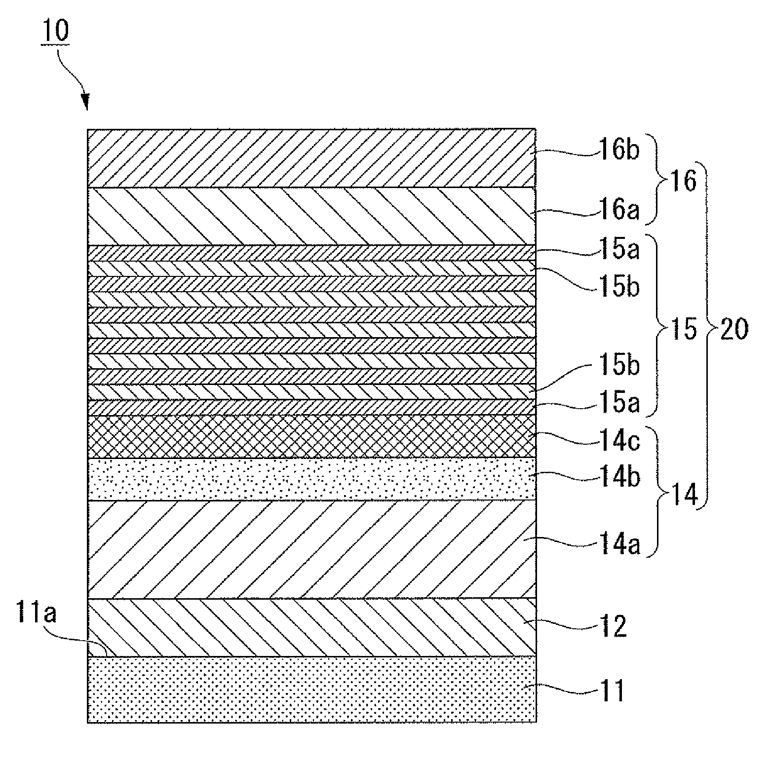
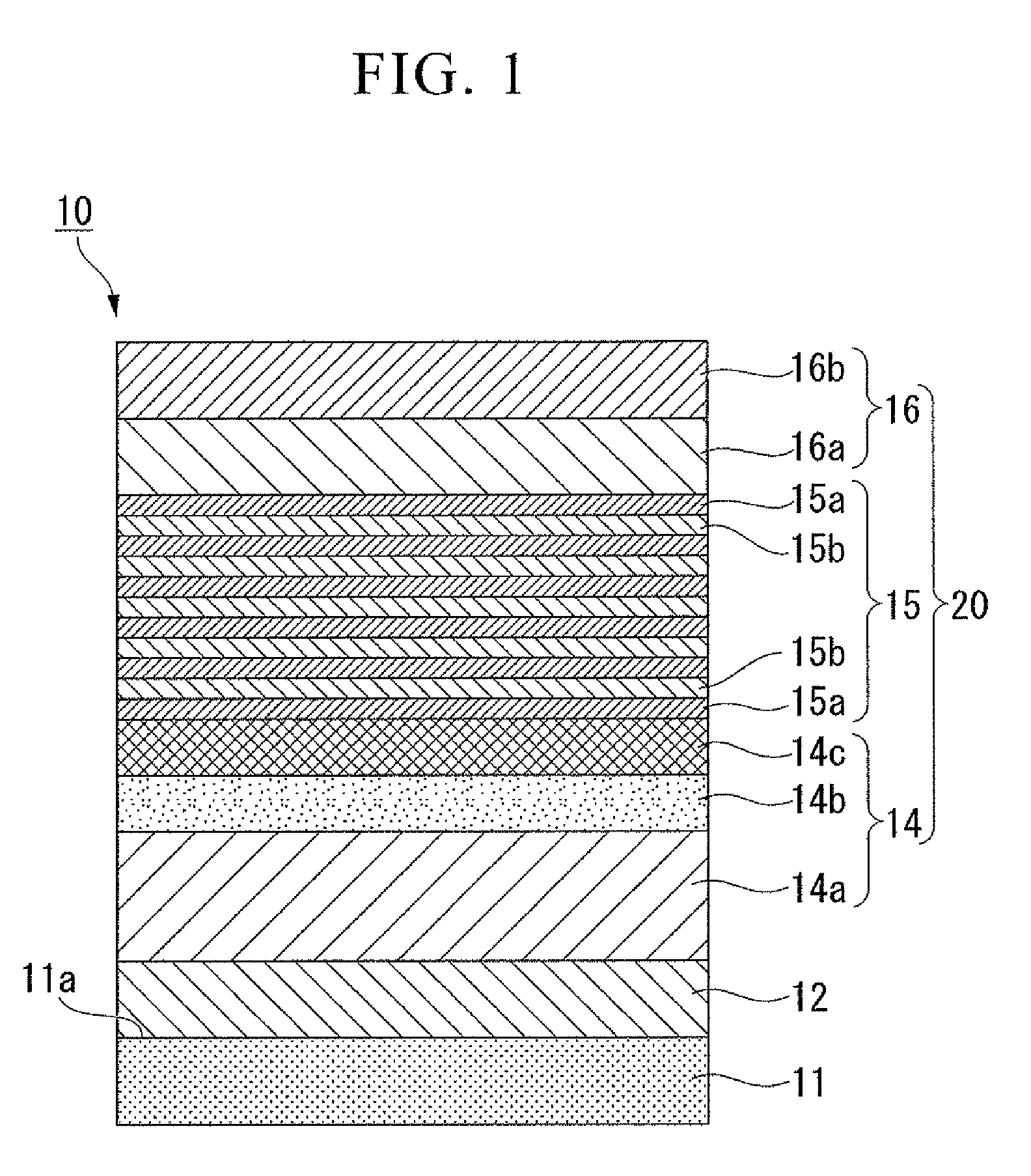
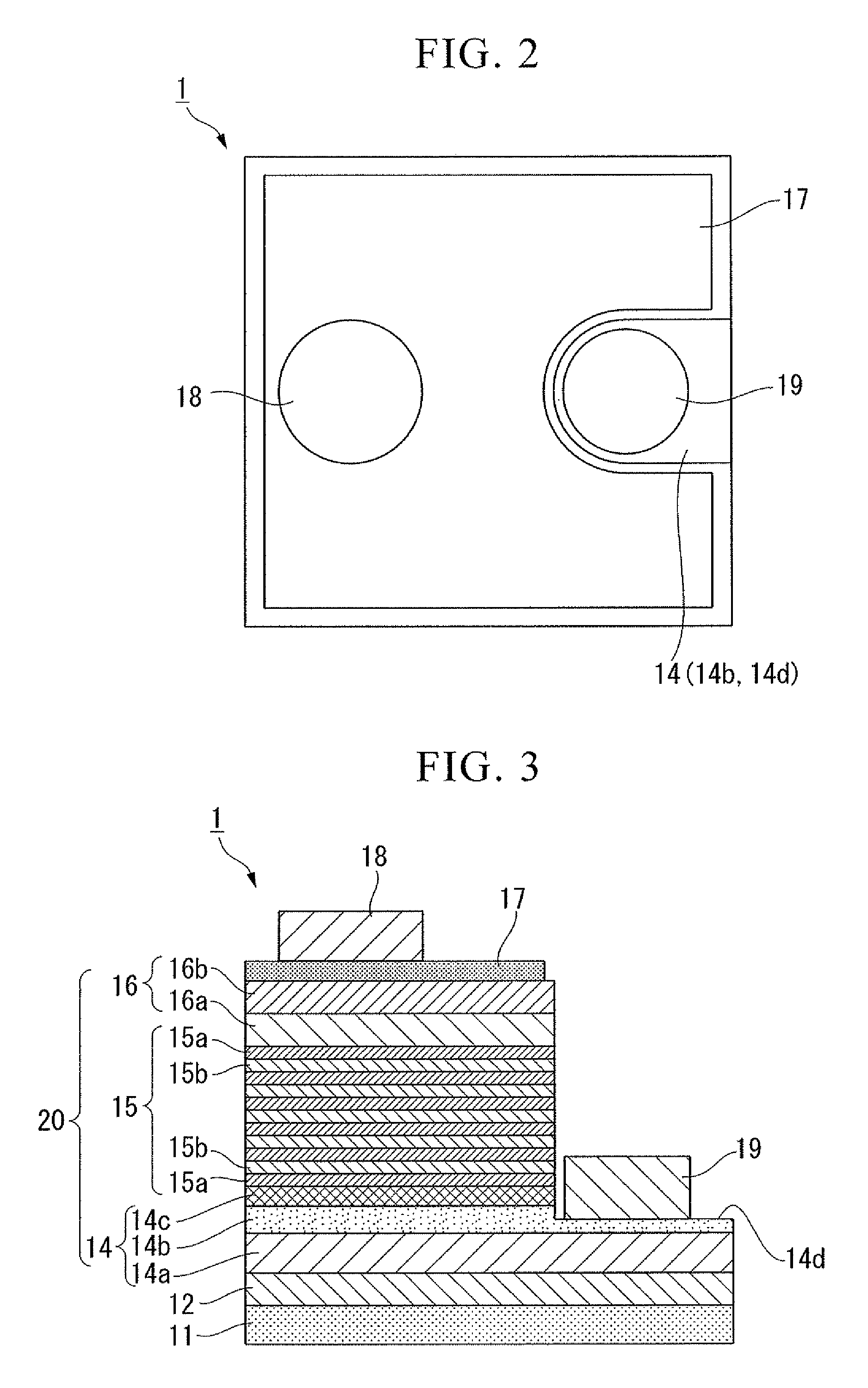
[0208]In Example 3, according to the same procedure as in Example 2, the buffer layer 12 was formed on the substrate 11, and then the ground layer 14a made of GaN was formed thereon. In addition, the respective layers were formed thereon according to the following procedure, to thereby produce the laminated semiconductor 10 represented by FIG. 1. Moreover, the transparent electrode 17, the positive electrode bonding pad 18, and the negative electrode 19 were formed for the laminated semiconductor 10, to thereby produce the light-emitting device 1 represented by FIGS. 2 and 3.
[Formation of N-Type Contact Layer]
[0209]According to the same procedure as in Example 2, the substrate 11 formed with the buffer layer 12 and the ground layer 14a was transported from the sputtering apparatus 40 into the chamber 41 of the other sputtering apparatus 40 having the same structure. As the sputtering apparatus 40 for use in the formation of the n-type contact layer 14b, there was employed the sputte...
PUM
| Property | Measurement | Unit |
|---|---|---|
| temperature T2 | aaaaa | aaaaa |
| temperature T2 | aaaaa | aaaaa |
| thickness t2 | aaaaa | aaaaa |
Abstract
Description
Claims
Application Information


