

Naphthalene derivative, resist bottom layer material, and patterning process
a bottom layer material and etching technology, applied in the field of naphthalene derivatives, can solve the problems of increasing surface roughness after etching to a serious concern, weak resistance of acrylate to substrate etching, and approaching the essential limit of resolution determined by the light source wavelength, etc., to achieve improved etching resistance, high heat resistance, and solvent resistance
- Summary
- Abstract
- Description
- Claims
- Application Information
AI Technical Summary
Benefits of technology
Problems solved by technology
Method used
Image

Examples
synthesis example 1
[0161]Synthesis of Naphthalene Derivative (I)
[0162]
(1-1)
[0163]A three-neck flask was charged with 15.9 g (5.6 mmol) of 1,1′-bi-2,2′-naphthol, 10.0 g (5.6 mmol) of 9-fluorenone, and 125 ml of 1,2-dichloroethane, which were dissolved by keeping the flask in an oil bath. After dissolution was confirmed, 0.3 ml of 3-mercaptopropionic acid and 3.0 ml of methanesulfonic acid were added dropwise. Under reflux, reaction was effected for 10 hours. At the end of reaction, the reaction solution was diluted with 300 ml of ethyl acetate, and transferred to a separatory funnel where it was washed with water and separated. Water washing was repeated until the water layer became neutral. The organic layer was concentrated under reduced pressure, and 100 ml of tetrahydrofuran (THF) was added to the residue, which was poured to 1,300 ml of hexane, allowing the polymer to crystallize. The crystallized polymer was collected by filtration and dried in vacuum, obtaining naphthalene derivative (I).
Naphtha...
synthesis example 2
[0170]Synthesis of Naphthalene Derivative (II)
[0171]
In the formulae, x and y each indicate a proportion of the corresponding partial structure.
(1-2)
[0172]A three-neck flask was charged with 7.9 g (2.8 mmol) of 1,1′-bi-2,2′-naphthol, 7.5 g (2.8 mmol) of 2,2′-dinaphthyl ether, 10.0 g (5.6 mmol) of 9-fluorenone, and 60 ml of 1,2-dichioroethane, which were dissolved by keeping the flask in an oil bath. After dissolution was confirmed, 0.3 ml of 3-mercaptopropionic acid and 3.0 ml of methanesulfonic acid were added dropwise. Under reflux, reaction was effected for 11 hours. At the end of reaction, the reaction solution was diluted with 100 ml of methyl isobutyl ketone and 100 ml of toluene, and transferred to a separatory funnel where it was washed with water and separated. Water washing was repeated until the water layer became neutral. The organic layer was concentrated under reduced pressure, and 140 ml of THF was added to the residue, which was poured to 1,500 ml of hexane, allowing ...
synthesis example 3
[0179]Synthesis of Naphthalene Derivative (III)
[0180]
(1-3)
[0181]A three-neck flask was charged with 24.87 g (86.8 mmol) of 1,1′-bi-2,2′-naphthol, 20.0 g (86.8 mmol) of 9-benzo[b]fluorenone, and 120 ml of 1,2-dichioroethane, which were dissolved by keeping the flask in an oil bath. After dissolution was confirmed, 0.60 ml of 3-mercaptopropionic acid and 6.0 ml of methanesulfonic acid were added dropwise. Under reflux, reaction was effected for 14 hours. At the end of reaction, the reaction solution was diluted with 500 ml of ethyl acetate, and transferred to a separatory funnel where it was washed with water and separated. Water washing was repeated until the water layer became neutral. The organic layer was concentrated under reduced pressure, and 200 ml of THF was added to the residue, which was poured to 1,500 ml of hexane, allowing the polymer to crystallize. The crystallized polymer was collected by filtration and dried in vacuum, obtaining naphthalene derivative (III).
Naphthale...
PUM
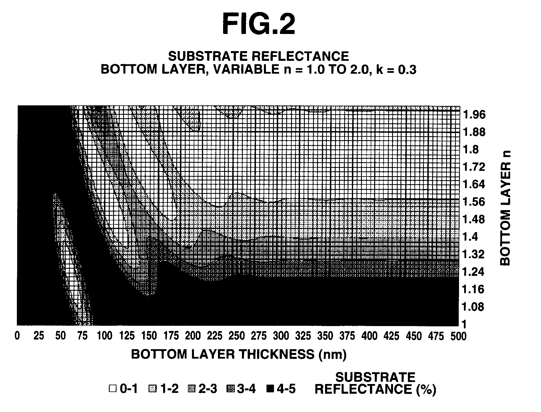
| Property | Measurement | Unit |
|---|---|---|
| wavelength | aaaaa | aaaaa |
| size | aaaaa | aaaaa |
| reflectance | aaaaa | aaaaa |
Abstract
Description
Claims
Application Information