Sputtering target, method for manufacturing the same, manufacturing semiconductor device

a technology of sputtering target and semiconductor device, which is applied in the direction of diaphragms, preheating charges, metallic material coating processes, etc., can solve the problems of preventing the formation of a compound having a desired nitrogen concentration in some cases, and the concentration of nitrogen is not high enough,

Inactive Publication Date: 2014-11-25
SEMICON ENERGY LAB CO LTD
View PDF149 Cites 11 Cited by
  • Summary
  • Abstract
  • Description
  • Claims
  • Application Information

AI Technical Summary

Benefits of technology

[0022]In particular, gallium and aluminum are easily combined with oxygen; thus, in formation of an oxynitride film by reactive sputtering with the use of an oxide containing gallium or aluminum, there is a great difficulty in substituting nitrogen for oxygen bonded to gallium or aluminum, so that the concentration of nitrogen becomes low.
[0031]In a sputtering target obtained according to at least one of the above embodiments of the present invention, nitrogen at a necessary concentration can be secured in advance. Therefore, the ratio of a heavy rare gas such as argon in a sputtering gas can be increased and productivity can be higher. This is preferable so that a highly conductive oxynitride whose concentration of nitrogen is particularly 4 atomic % or more, especially 20 atomic % or more is efficiently obtained. Needless to say, nitrogen may be contained in an atmosphere at the time of sputtering.
[0032]Further, when the concentrations of impurities such as hydrogen, an alkali metal, and an alkaline earth metal in a sputtering target are reduced, the reliability of a semiconductor device to be obtained can be increased. In particular, the density of carriers in an oxide semiconductor film has an influence on the threshold voltage of a transistor including an oxide semiconductor.
[0033]The carriers in the oxide semiconductor film are also generated from impurities contained in the oxide semiconductor film. For example, impurities such as a compound containing a hydrogen atom typified by water (H2O), a compound containing an alkali metal, or a compound containing an alkaline earth metal contained in the deposited oxide semiconductor film increase the carrier density of the oxide semiconductor film.
[0041]This is preferable particularly in the case of manufacturing a semiconductor device (e.g., a transistor) including an oxide semiconductor such as an In—Ga—Zn—O-based compound. For example, by taking advantage of a work function larger than those of metals which can be usually used, the threshold voltage of the transistor can be higher and the transistor can become normally off.
[0044]Such a difference corresponds to a p-n junction in a general silicon MOS transistor, and is substantially the same as, specifically, a junction between a channel and an extension region of a silicon MOS transistor which is doped at a high concentration, which means that the difference is effective in suppressing a short channel effect. In a transistor in which an oxide semiconductor is used for a channel and the channel length is 20 nm or less, an In—Ga—Zn—O—N-based compound is preferably used for a material to be in contact with the channel.

Problems solved by technology

However, in the case of employing reactive sputtering, when the ratio of nitrogen in an atmosphere is decreased, the concentration of nitrogen in an In—Ga—Zn—O—N-based compound to be obtained becomes low, which prevents formation of a compound having a desired concentration of nitrogen in some cases.
In particular, it is difficult to stably obtain an In—Ga—Zn—O—N-based compound whose concentration of nitrogen is 20 atomic % or more by reactive sputtering.

Method used


Image

  • Sputtering target, method for manufacturing the same, manufacturing semiconductor device
  • Sputtering target, method for manufacturing the same, manufacturing semiconductor device
  • Sputtering target, method for manufacturing the same, manufacturing semiconductor device

Examples


embodiment 1

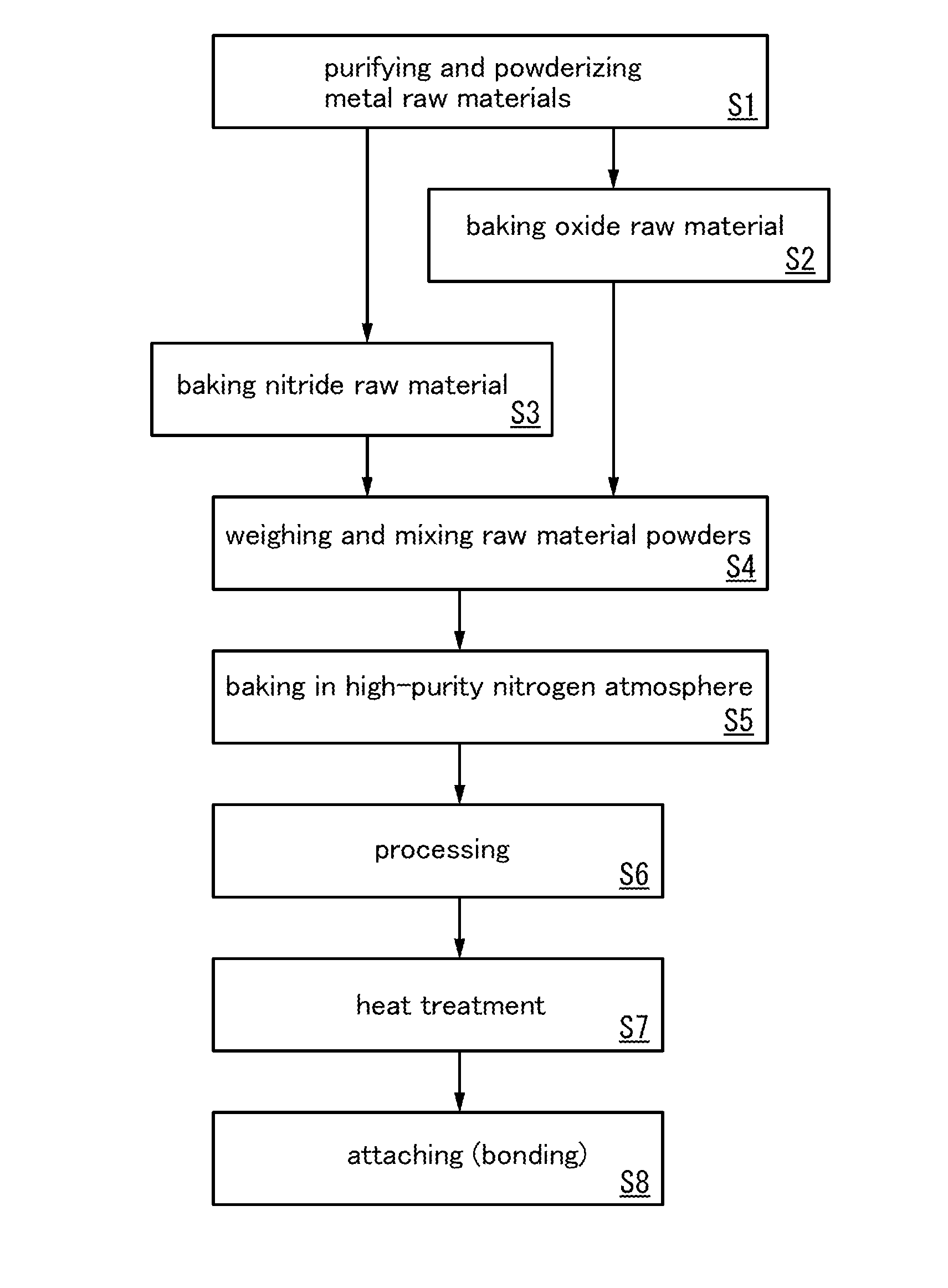
[0061]In this embodiment, a method for manufacturing a sputtering target which is one embodiment of the present invention will be described with reference to FIG. 1. FIG. 1 is a flow chart illustrating an example of a method for manufacturing a sputtering target according to this embodiment. Although manufacture of a sputtering target of an In—Ga—Zn—O—N-based compound is described below, manufacture of a sputtering target of another oxynitride can be performed similarly.

[0062]Here, a case is described where a sputtering target is formed by baking indium nitride, gallium nitride, indium oxide, gallium oxide, and zinc oxide as raw materials. First, zinc, indium, and gallium are each purified by repeating distillation, sublimation, or recrystallization. The purity of each of the materials is made 99.99% or more, preferably 99.9999% or more. After that, the purified metals are each processed into a powder form (S1).

[0063]Metal zinc, metal indium, and metal gallium which are highly purif...

embodiment 2

[0083]In this embodiment, one embodiment of a semiconductor device and a method for manufacturing the semiconductor device will be described with reference to FIGS. 3A to 3C, FIGS. 4A and 4B, and FIGS. 5A to 5E.

[0084]FIGS. 3A to 3C are a top view and cross-sectional views illustrating a transistor 151 which is a top-gate top-contact type as an example of a semiconductor device according to one embodiment of the present invention. Here, FIG. 3A is a top view, FIG. 3B is a cross-sectional view along A-B of FIG. 3A, and FIG. 3C is a cross-sectional view along C-D of FIG. 3A. Note that in FIG. 3A, some of components of the transistor 151 (for example, a gate insulating layer 112) are omitted for brevity.

[0085]The transistor 151 in FIGS. 3A to 3C includes an insulating layer 102, an oxide semiconductor layer 106, a source electrode 108a, a drain electrode 108b, the gate insulating layer 112, a first gate electrode layer 114, and a second gate electrode layer 115 over a substrate 100.

[008...

embodiment 3

[0163]In this embodiment, an example of a manufacturing process of the transistor 152 in FIG. 4A will be described below with reference to FIGS. 6A to 6E.

[0164]First, the insulating layer 102 is formed over the substrate 100 (see FIG. 6A). Next, a conductive layer for forming of the source electrode and the drain electrode (including a wiring formed in the same layer as the source electrode and the drain electrode) is formed over the insulating layer 102 and processed to form the source electrode 108a and the drain electrode 108b (see FIG. 6B).

[0165]Next, an oxide semiconductor layer connected to the source electrode 108a and the drain electrode 108b is formed over the insulating layer 102 and then is processed to form the oxide semiconductor layer 106 having an island shape (see FIG. 6C). After that, first heat treatment similar to that performed on the transistor 151 may be performed.

[0166]Next, the gate insulating layer 112 is formed so as to cover the source electrode 108a and t...


PUM

PropertyMeasurementUnit
lengthaaaaaaaaaa
gate potentialaaaaaaaaaa
lengthaaaaaaaaaa

Abstract

A deposition technique for forming an oxynitride film is provided. A highly reliable semiconductor element is manufactured with the use of the oxynitride film. The oxynitride film is formed with the use of a sputtering target including an oxynitride containing indium, gallium, and zinc, which is obtained by sintering a mixture of at least one of indium nitride, gallium nitride, and zinc nitride as a raw material and at least one of indium oxide, gallium oxide, and zinc oxide in a nitrogen atmosphere. In this manner, the oxynitride film can contain nitrogen at a necessary concentration. The oxynitride film can be used for a gate, a source electrode, a drain electrode, or the like of a transistor.

Description

BACKGROUND OF THE INVENTION[0001]1. Field of the Invention[0002]The present invention relates to a sputtering target and a method for manufacturing the sputtering target. Further, the present invention relates to a method for manufacturing a semiconductor device with the use of the sputtering target. In this specification, a semiconductor device means a general device which can function by utilizing semiconductor characteristics, and an electro-optic device, a semiconductor circuit, and an electronic device are all semiconductor devices.[0003]2. Description of the Related Art[0004]A transistor formed over a flat plate such as a glass substrate, which is typically used in a liquid crystal display device, is generally formed using a semiconductor material such as amorphous silicon or polycrystalline silicon. A transistor manufactured using amorphous silicon has low field effect mobility, but can be formed over a larger glass substrate. In contrast, a transistor manufactured using poly...

Claims


Application Information

Patent Timeline
Patent Type & Authority Patents(United States)
IPC IPC(8): C23C14/14
CPCC23C14/3414C04B35/453C04B2235/77C04B35/58C04B2235/3284C04B2235/3852C04B35/6455C04B2235/3286C23C14/0676C04B2235/666H01L21/443H01L21/02565H01L29/4966H01L29/4908C23C14/34H01L21/20H01L21/02631
Inventor YAMAZAKI, SHUNPEI
Owner SEMICON ENERGY LAB CO LTD
Why Eureka
Try Eureka