

Resist underlayer film forming composition containing phenylindole-containing novolac resin
a technology of resist film and composition, which is applied in the field of resist film forming composition for lithography, can solve the problems of difficult to obtain a sufficient resist pattern film thickness in substrate processing, and difficulty in obtaining a sufficient resist pattern film thickness, so as to achieve sufficient etching resistance, excellent resist pattern shape, and reduced reflection
- Summary
- Abstract
- Description
- Claims
- Application Information
AI Technical Summary
Benefits of technology
Problems solved by technology
Method used
Image

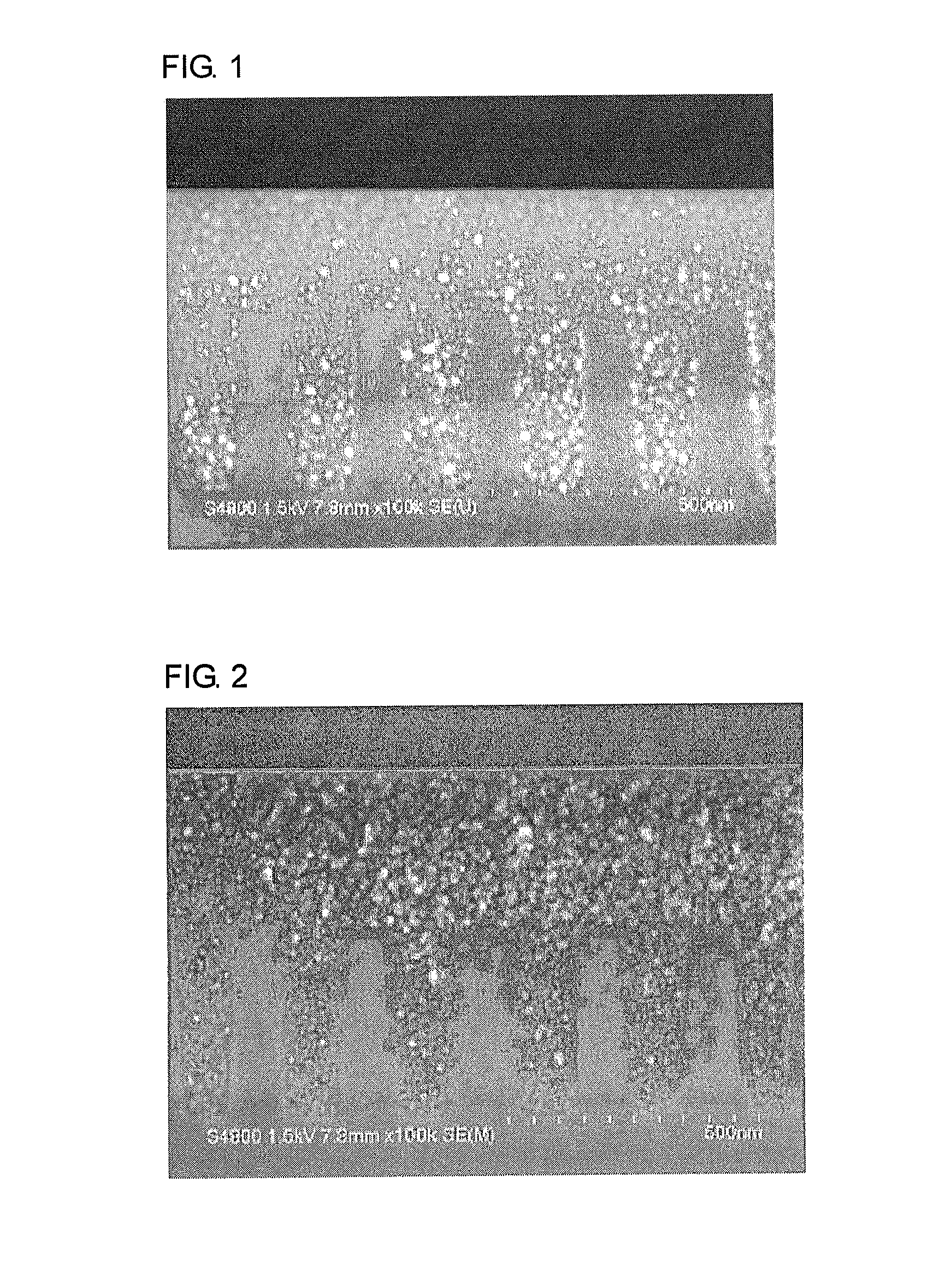
Examples
synthesis example 1
[0110]To a 100 mL four-necked flask, 2-phenylindole (4.00 g, 0.021 mol, manufactured by Tokyo Chemical Industry Co., Ltd.), 1-naphthaldehyde (3.23 g, 0.021 mol, manufactured by Tokyo Chemical Industry Co., Ltd.), and p-toluene sulfonic acid monohydrate (0.619 g, 0.0031 mol, manufactured by KANTO CHEMICAL CO., INC.) were added and then toluene (14.58 g, manufactured by KANTO CHEMICAL CO., INC.) was charged. The mixture was stirred and a temperature of the mixture rose to 110° C. to dissolve the mixture and to start polymerization. After 50 minutes, the resulting mixture was allowed to cool to room temperature and was reprecipitated in methanol (300 g, manufactured by KANTO CHEMICAL CO., INC.). The obtained precipitate was filtered and dried at 50° C. for 10 hours in a vacuum drier to obtain 4.5 g of a target polymer (Formula (2-2), hereinafter abbreviated as PId-NA).
[0111]A weight average molecular weight Mw and a polydispersity Mw / Mn of PId-NA measured by GPC in terms of polystyrene...
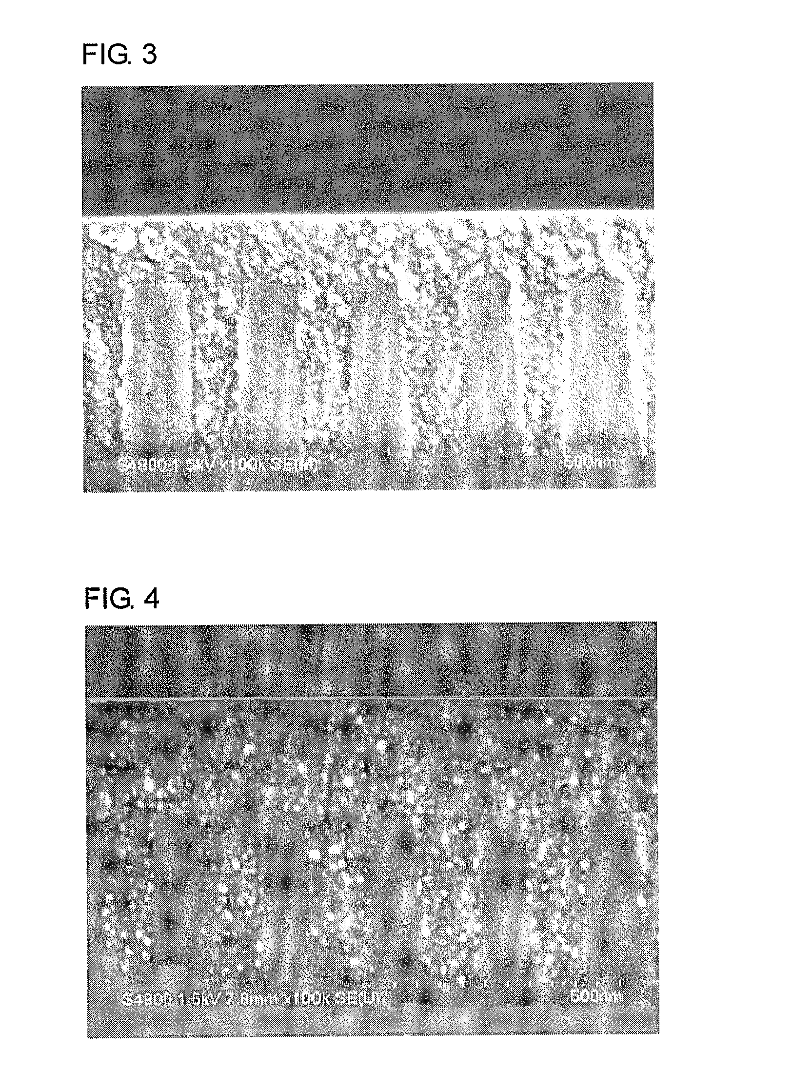
synthesis example 2
[0112]To a 100 mL four-necked flask, 2-phenylindole (3.50 g, 0.018 mol, manufactured by Tokyo Chemical Industry Co., Ltd.), 1-pyrene-carboxaldehyde (4.17 g, 0.018 mol, manufactured by Tokyo Chemical Industry Co., Ltd.), and p-toluene sulfonic acid monohydrate (0.541 g, 0.0027 mol, manufactured by KANTO CHEMICAL CO., INC.) were added and then 1,4-dixoane (15.25 g, manufactured by KANTO CHEMICAL CO., INC.) was charged. The mixture was stirred and a temperature of the mixture rose to 110° C. to dissolve the mixture and to start polymerization. After 24 hours, the resulting mixture was allowed to cool to room temperature and was reprecipitated in methanol (250 g, manufactured by KANTO CHEMICAL CO., INC.). The obtained precipitate was filtered and dried at 50° C. for 10 hours and further 120° C. for 24 hours in a vacuum drier to obtain 3.7 g of a target polymer (Formula (2-7), hereinafter abbreviated as PId-Py).
[0113]A weight average molecular weight Mw and a polydispersity Mw / Mn of PId-...
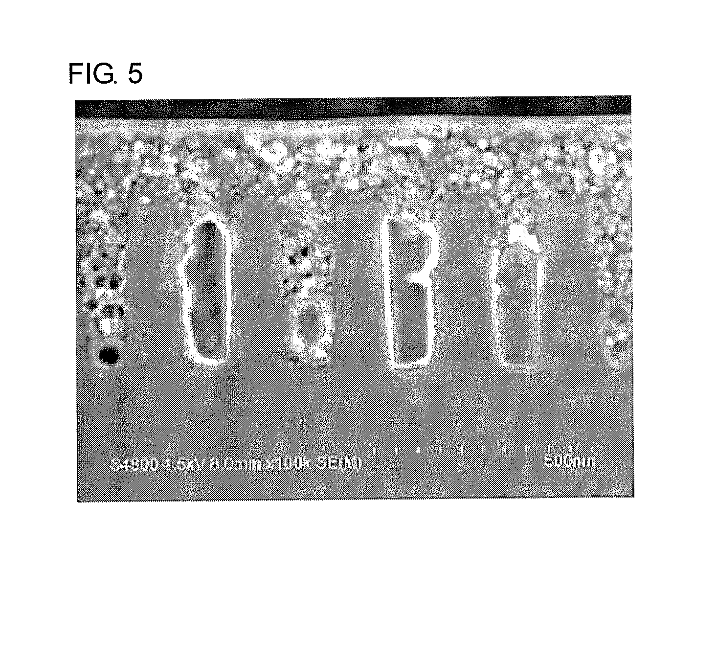
example 1
[0117]With 20 g of the resin obtained in Synthesis Example 1, 0.06 g of Megafac R-30 (trade name, manufactured by Dainippon Ink and Chemicals Co., Ltd.) as the surfactant was mixed and the mixture was dissolved in 80 g of propylene glycol monomethyl ether acetate to form a solution. Thereafter, the solution was filtered with a polyethylene microfilter having a pore diameter of 0.10 μm and further filtered with a polyethylene microfilter having a pore diameter of 0.05 μm to prepare a solution of a resist underlayer film forming composition used for a lithography process of a multilayer film.
PUM
| Property | Measurement | Unit |
|---|---|---|
| wavelengths | aaaaa | aaaaa |
| wavelengths | aaaaa | aaaaa |
| wavelengths | aaaaa | aaaaa |
Abstract
Description
Claims
Application Information