Micro-mechanical wafer chip test detecting card and its production

A chip testing, wafer-level technology, used in semiconductor/solid-state device testing/measurement, electrical measurement, measurement devices, etc., to solve problems such as limiting work performance, difficult to test signal transmission analysis, and probe array flatness effects. , to achieve the effect of simplifying the manufacturing process, high probe flatness, and simplifying the process steps

Inactive Publication Date: 2009-04-15
深圳市道格特科技有限公司
View PDF6 Cites 0 Cited by
  • Summary
  • Abstract
  • Description
  • Claims
  • Application Information

AI Technical Summary

Problems solved by technology

However, due to the stress gradient in the electroplated metal layer, the flatness of the probe array is affected, which greatly limits the working performance.
On the other hand, if the entire probe card structure is made of single crystal silicon, although the flatness of the probe can be greatly improved, it is difficult to transmit the test signal from the probe tip to the test instrument for analysis (Dong-il Cho et. al, "Probe structure for testing semiconductor devices and method for fabricating the same," US Patent 6,724,204, 2004.)

Method used


Image

  • Micro-mechanical wafer chip test detecting card and its production
  • Micro-mechanical wafer chip test detecting card and its production
  • Micro-mechanical wafer chip test detecting card and its production

Examples


Embodiment 1

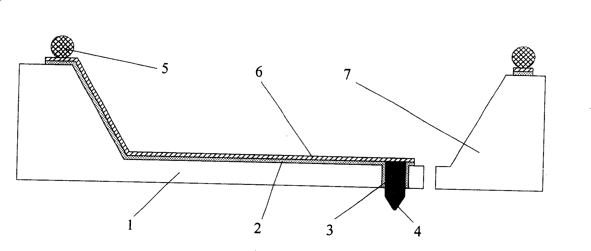
[0076] 1. Deposit or oxidize a 1.5-2.5 μm thick oxide layer 8 on the front and back sides of (100) double-sided polished silicon wafer 7 as an etching mask, and use 50 ° C and 40% KOH solution to etch the etching window. About 300 μm, the thickness of the reserved silicon film 9 is the sum of the thickness of the cantilever beam and the height of the probe ( image 3 );

[0077] 2. The oxide layer 8 on the back side of the photolithographic silicon wafer 7 is used as a mask, and the silicon film 9 is etched to form interconnection holes 10 ( Figure 4 );

[0078] 3. Remove the oxide layer 8 on the surface of the silicon wafer 7, and oxidize and generate 2.0 μm thick SiO on the surface of the silicon wafer and interconnect holes 2 Insulating layer 2, sputtering 5000 on the upper surface of the silicon wafer Titanium copper metal layer 11 ( Figure 5 );

[0079] 4. Spray glue on the front side of the silicon wafer 7 and photoetch a 10 μm thick photoresist mask 12, and use ...

Embodiment 2

[0086] 1. Same as in Example 1, deposit or oxidize a 1.5-2.5 μm thick oxide layer 8 on both sides of the (100) double-sided polished silicon wafer 7 as an etching mask, and use 50° C. and 40% KOH solution to etch the window by photolithography Etching is carried out, the etching depth is about 300 μm, and the thickness of the remaining silicon film 9 is the sum of the thickness of the cantilever beam and the height of the probe ( image 3 );

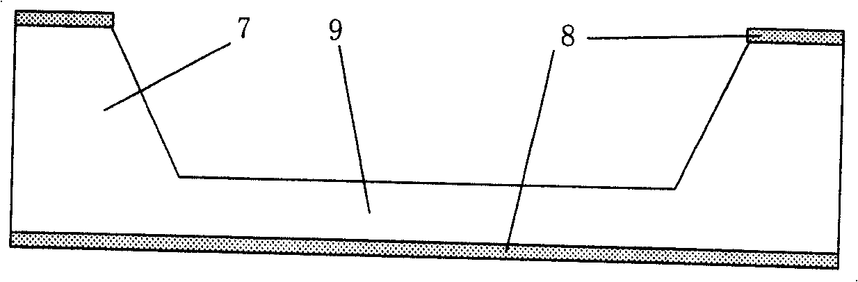
[0087] 2. Deposit or oxidize 5000 Oxide layer, utilize glue-spray photolithography to form etching window 19, carry out second time KOH etching, form inverted pyramid shape 20 ( Figure 12 );

[0088] 3. Use reactive ion etching to etch through the silicon film 9 from top to bottom to form interconnection holes 21 with a needle point shape, and then oxidize the surface of the silicon wafer 7 to form SiO with a thickness of 2 μm 2 Insulation layer 2 ( Figure 13 );

[0089] 4. Take another piece of silicon wafer as the adhesive shee...


PUM

PropertyMeasurementUnit
diameteraaaaaaaaaa

Abstract

The invention is concerned with tiny engine wafer level chip testing probe and its production, relating to probe, pinpoint, cantilever beam, signal line and packaging solder ball. The pinpoint is at the end of cantilever beam and insets in the interconnecting hole, while the other end of cantilever beam connects with silicon. The pinpoint and packaging solder ball are at the up and down sides of wafer. Signal line sets on the upper surface of cantilever beam and the cant of corrosion groove, and the position arrangement of cantilever beam of the probe is according to the place distribution of tested chip. Produce the interconnecting hole to signal of the face and back and the pinpoint at the same time in the way from up to down or from down to up, and show up pinpoint at the time of releasing cantilever beam. The probe has excellent plane and is easy to encapsulation seal with PCB circuit board.

Description

technical field [0001] The invention relates to a wafer-level chip test probe card and a manufacturing method based on a micro-mechanical method, belonging to the field of micro-electro-mechanical systems. Background technique [0002] At present, semiconductor manufacturing technology is developing rapidly in our country. The complexity of integrated circuits continues to increase, chip sizes are getting smaller and smaller, and device functions are becoming more and more complex. In the production cost of the entire chip, the chip packaging cost occupies a large proportion. Wafer-level chip testing is a preliminary test before chip packaging, thereby greatly reducing packaging costs. Probing cards are a central element in this testing process. However, with the continuous improvement of the chip manufacturing process, there are more and more pins on the chip, and the distance between the pins is getting smaller and smaller. At the same time, the operating frequency of ...

Claims


Application Information

Patent Timeline
Patent Type & Authority Patents(China)
IPC IPC(8): H01L21/66B81B7/02B81C1/00G01R1/073G01R3/00
Inventor 李昕欣汪飞
Owner 深圳市道格特科技有限公司
Why Eureka
Try Eureka