

Ceramic coating member for semiconductor processing apparatus
A technology for processing devices and covering parts, applied in semiconductor/solid-state device manufacturing, superimposed layer plating, electrical components, etc., can solve problems such as corrosive environments and instrument damage, and achieve improved plasma output, increased productivity, and light weight The effect of the improved
- Summary
- Abstract
- Description
- Claims
- Application Information
AI Technical Summary
Problems solved by technology
Method used
Image

Examples
experiment example 1
[0076] In this experimental example, the state of sputtered film formation of Group IIIB element oxides, and the state of the layer formed when electron beam irradiation and laser beam irradiation were performed on the obtained film were investigated. In addition, Sc 2 o 3 , Y 2 o 3 , La 2 o 3 , CeO 2 、Eu 2 o 3 、Dy 2 o 3 and Yb 2 o 3 Seven kinds of oxide powders (average particle size: 10-50 μm). Then, these powders are directly sprayed with a thickness of 100 μm by atmospheric plasma spraying (APS) and reduced pressure plasma spraying (LPPS) on one side of an aluminum test piece (size: width 50mm x length 60mm x thickness 8mm). coating. Then, the surfaces of these films were subjected to electron beam irradiation treatment and laser beam irradiation treatment. Table 1 summarizes the results of this experiment.
[0077] In addition, the actual results of the spraying of lanthanide metal oxides with atomic numbers from 57 to 71 have not been reported so far. Ther...
experiment example 2
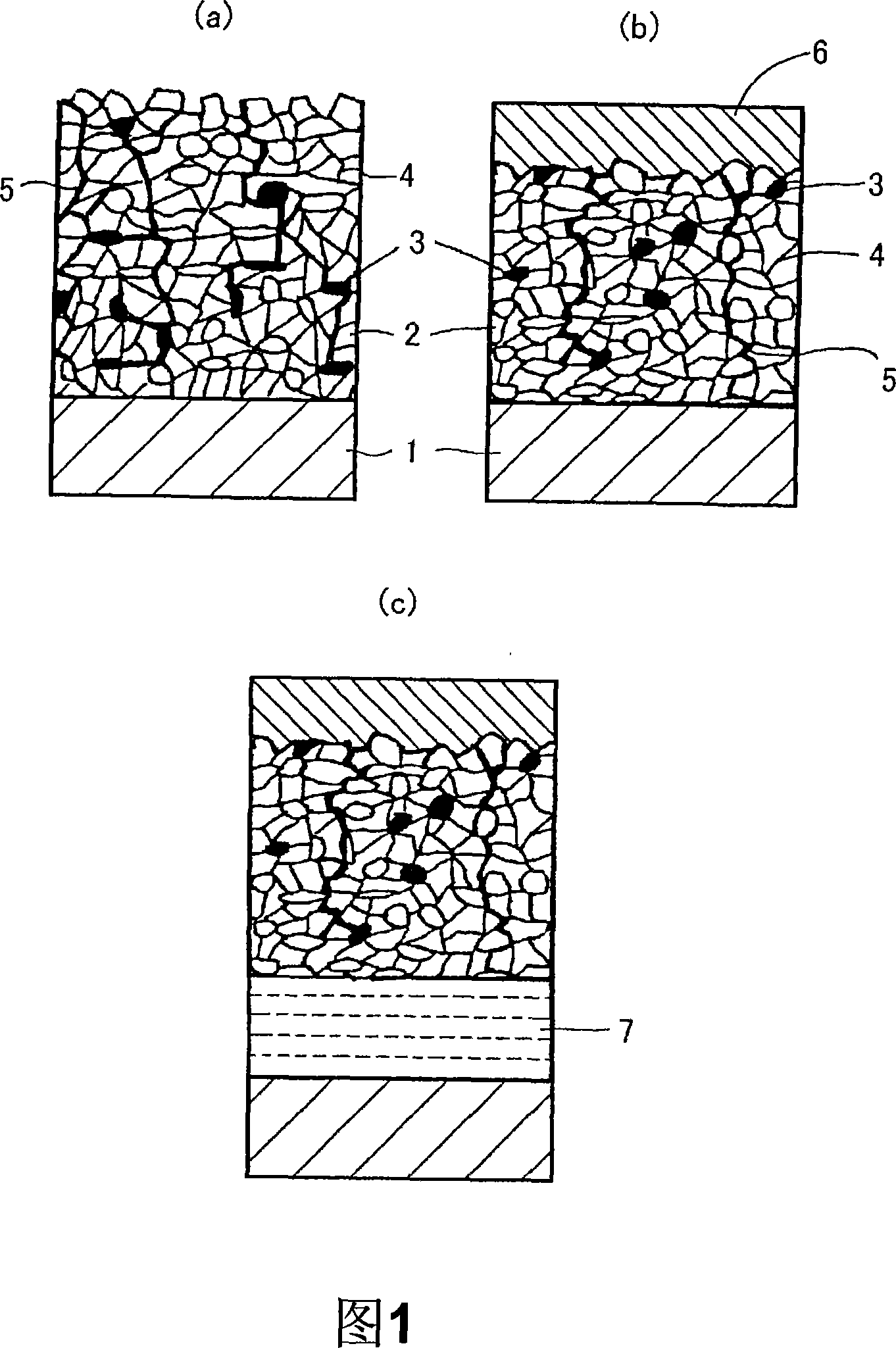
[0084] In this experimental example, from the test piece after the high-energy irradiation treatment made in the above-mentioned test 1, for Y 2 o 3 For the sprayed coating, observe the section of the sprayed coating before and after the electron beam irradiation treatment with an optical microscope, and observe the changes in the microstructure of the film produced by the high-energy irradiation treatment.
[0085] Figure 1 is a schematic representation of Y 2 o 3 Changes in the microstructure near the surface of a thermally sprayed film (porous film), a film subjected to electron beam irradiation treatment, and a composite film with an undercoat layer. In the non-irradiation-treated test piece shown in FIG. 1( a ), it can be seen that the sprayed particles constituting the film exist independently, and the surface roughness is large. On the other hand, FIG. 1( b ) shows that a new layer having a different microstructure is formed on the above-mentioned sprayed coating by ...
experiment example 3
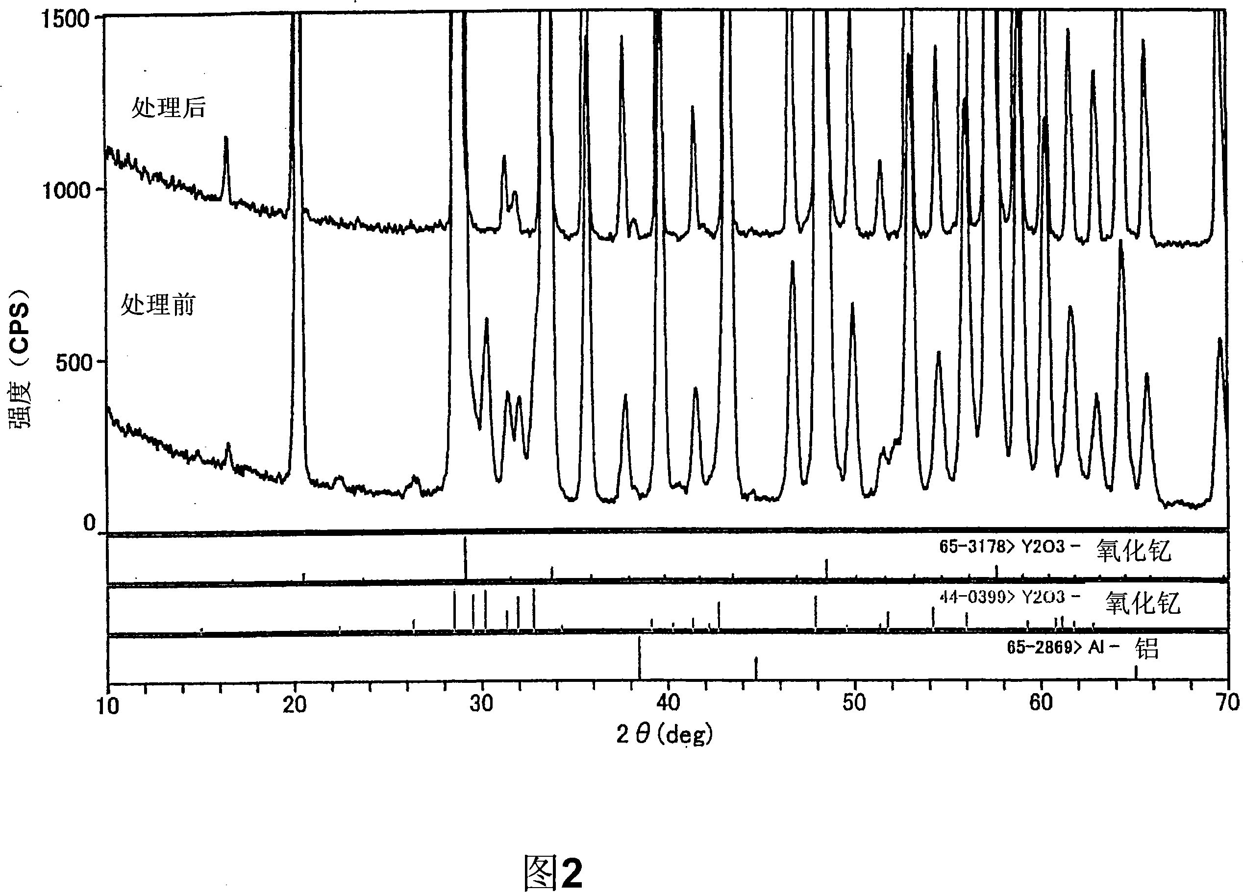
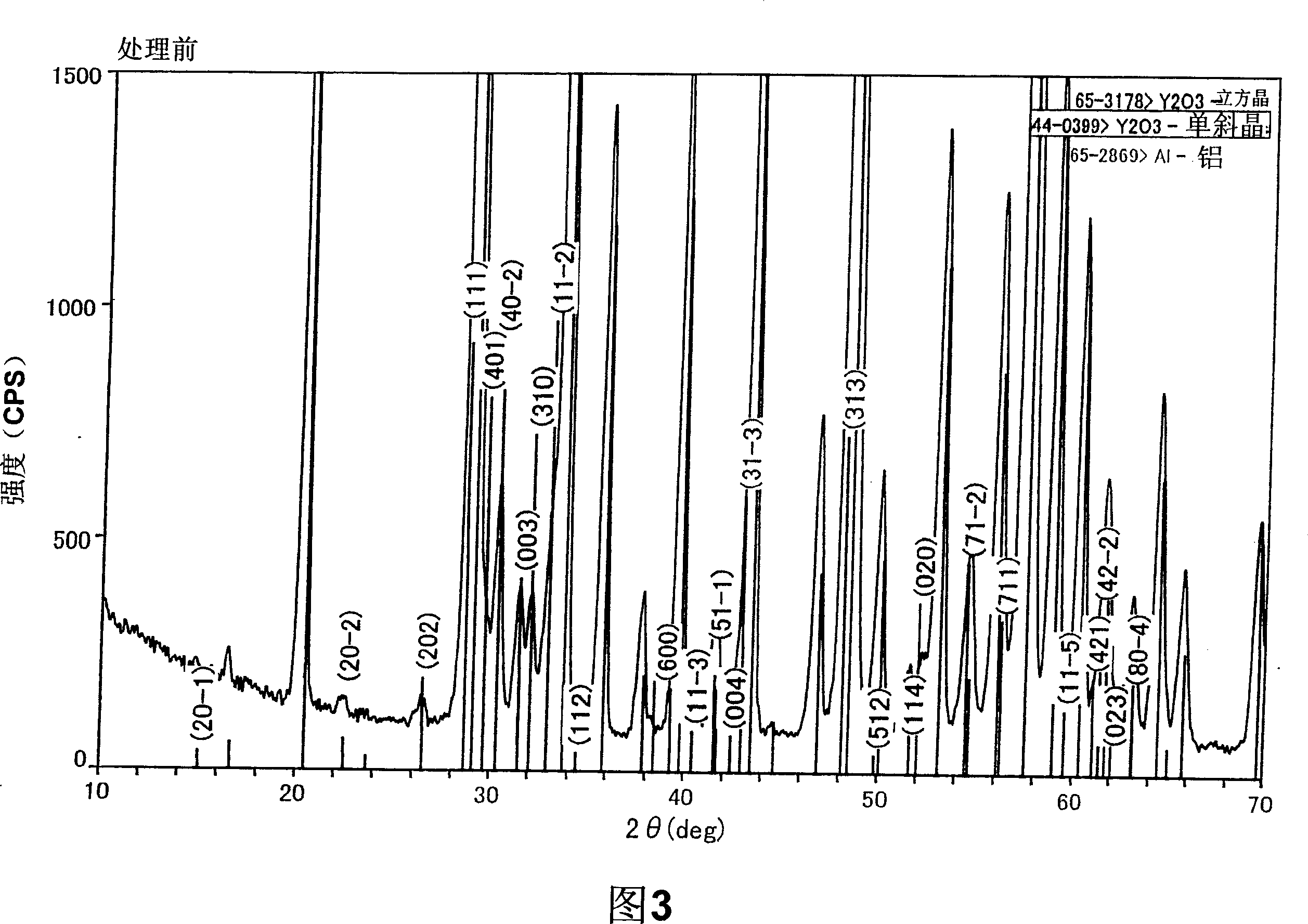
[0088] In this experimental example, the Y in Figure 1(a) was determined by XRD 2 o 3 The porous layer of the thermally sprayed film and the secondary recrystallized layer shown in FIG. 1( b ) produced by electron beam irradiation under the following conditions were studied for the crystal structure of each layer. This result is shown in FIG. 2 , showing an XRD pattern before the electron beam irradiation treatment. In addition, FIG. 3 is an X-ray diffraction diagram on the vertical axis before the enlargement process. Fig. 4 is an X-ray diffraction diagram of the vertical axis after enlargement processing. As can be seen from FIG. 3 , in the sample before treatment, a peak indicating a monoclinic crystal was observed particularly in the range of 30° to 35°, and the cubic crystal and monoclinic crystal were in a mixed state. In contrast, as shown in Figure 4, denoting Y 2 o 3 The peaks of the particles become sharper, the peaks of monoclinic crystals attenuate, and the pl...
PUM
| Property | Measurement | Unit |
|---|---|---|
| porosity | aaaaa | aaaaa |
| surface roughness | aaaaa | aaaaa |
| mean roughness | aaaaa | aaaaa |
Abstract
Description
Claims
Application Information