Wideband gap gallium nitride radical heterojunction field effect transistor structure and method for making

A heterojunction field effect, gap gallium nitride based technology, applied in semiconductor/solid state device manufacturing, semiconductor devices, electrical components, etc. Reduce the lattice integrity of materials and other problems to achieve the effect of reducing defect density, improving crystal quality, and relieving stress

Inactive Publication Date: 2008-03-05
INST OF SEMICONDUCTORS - CHINESE ACAD OF SCI
View PDF0 Cites 36 Cited by
  • Summary
  • Abstract
  • Description
  • Claims
  • Application Information

AI Technical Summary

Problems solved by technology

However, doping will reduce the integrity of the material lattice, resulting in a decrease in the crystal quality of the AlGaN layer, a

Method used


Image

  • Wideband gap gallium nitride radical heterojunction field effect transistor structure and method for making
  • Wideband gap gallium nitride radical heterojunction field effect transistor structure and method for making

Examples


Embodiment

[0107] The specific growth temperature, growth pressure and growth thickness of each growth layer of the gallium nitride-based heterojunction field effect transistor structure of the present invention are shown in Table 1:

[0108] Table 1

[0109] growth layer name

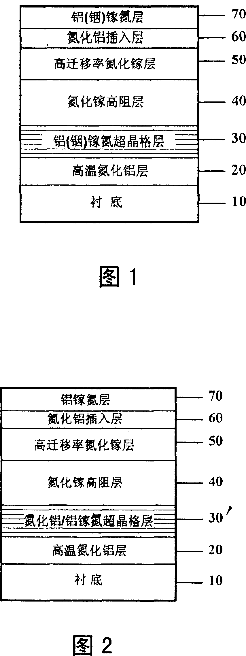
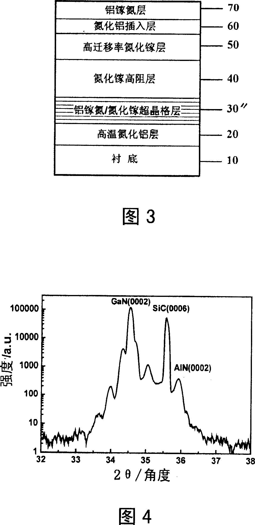
[0110] Figure 2 and Figure 3 show two preferred specific embodiments of the HEMT formed according to the present invention, including:

[0111] A substrate 10, preferably silicon carbide and silicon substrates with high thermal conductivity, especially silicon carbide substrates with a small lattice mismatch with gallium nitride, wherein the silicon carbide substrates include but are not limited to semi-insulating or conductive 4H Silicon carbide substrate or semi-insulating or conductive 6H silicon carbide substrate;

[0112] A high-temperature aluminum nitride nucleation layer 20, the high-temperature aluminum nitride nucleation layer 20 is fabricated on the silicon carbide substrate 10

[0113] An ...


PUM

PropertyMeasurementUnit
Thicknessaaaaaaaaaa
Thicknessaaaaaaaaaa
Thicknessaaaaaaaaaa

Abstract

This invention relates to a wide band-gap GaN-base heterojunction field effect transistor structure including: a substrate, a high temperature AlN nucleating layer on the substrate, an AlInGaN supper lattice buffer layer processed on the nucleating layer, a non-intentional or intentional doped GaN high resist layer processed on the buffer layer, a non-intentional doped high transfer rate GaN layer processed on the high resist layer and an AlN insertion layer set on the high transfer rate GaN layer and a non-intentional doped or n-type doped AlInGaN layer set on the AlN insertion layer.

Description

technical field [0001] The invention belongs to the technical field of semiconductors, in particular to a gallium nitride-based heterojunction field effect transistor structure using a superlattice structure buffer layer and a high-mobility gallium nitride channel layer and a manufacturing method thereof, which can significantly reduce the material Lattice defects and enhanced channel two-dimensional electron gas mobility. Background technique [0002] As a typical representative of the third-generation wide-bandgap semiconductor, gallium nitride has excellent thermal and chemical stability, high breakdown voltage, high electron saturation drift velocity and excellent radiation resistance, and is especially suitable for the preparation of high temperature, high Heterojunction field effect transistors with high frequency, high power and radiation resistance. Gallium nitride-based heterojunction field effect transistors have broad application prospects in wireless communicati...

Claims


Application Information

Patent Timeline
IPC IPC(8): H01L29/778H01L21/335
Inventor 王晓亮马志勇胡国新肖红领冉军学王翠梅罗卫军
Owner INST OF SEMICONDUCTORS - CHINESE ACAD OF SCI
Why Eureka
Try Eureka