Material with metal silicide nanostructure and method for making the same

A technology of metal silicide and nanostructure, applied in semiconductor/solid-state device manufacturing, electrical components, electrical solid-state devices, etc., can solve the problems of difficult control of size, shape and growth position, achieve low power consumption and eliminate latch-up effect , The effect of simple production process

Inactive Publication Date: 2008-06-25
INST OF PHYSICS - CHINESE ACAD OF SCI
View PDF0 Cites 14 Cited by
  • Summary
  • Abstract
  • Description
  • Claims
  • Application Information

AI Technical Summary

Problems solved by technology

[0006] The purpose of the present invention is to: overcome the shortcomings of the size, shape and growth position that are not easy to control in the existing methods for preparing metal silicide nanostructures, and provide a material and preparation method for making metal silicide nanostructures on SOI substrates. method, the fabricated metal silicide nanostructure is compatible with the current integrated circuit manufacturing process, not only applicable to the fabrication of interconnection wires and electrodes in integrated circuits, but also can be used to study the physical and chemical properties of these nanostructures themselves; this method has the potential to controlled size, shape and growth position

Method used


Image

  • Material with metal silicide nanostructure and method for making the same
  • Material with metal silicide nanostructure and method for making the same

Examples


Embodiment 1

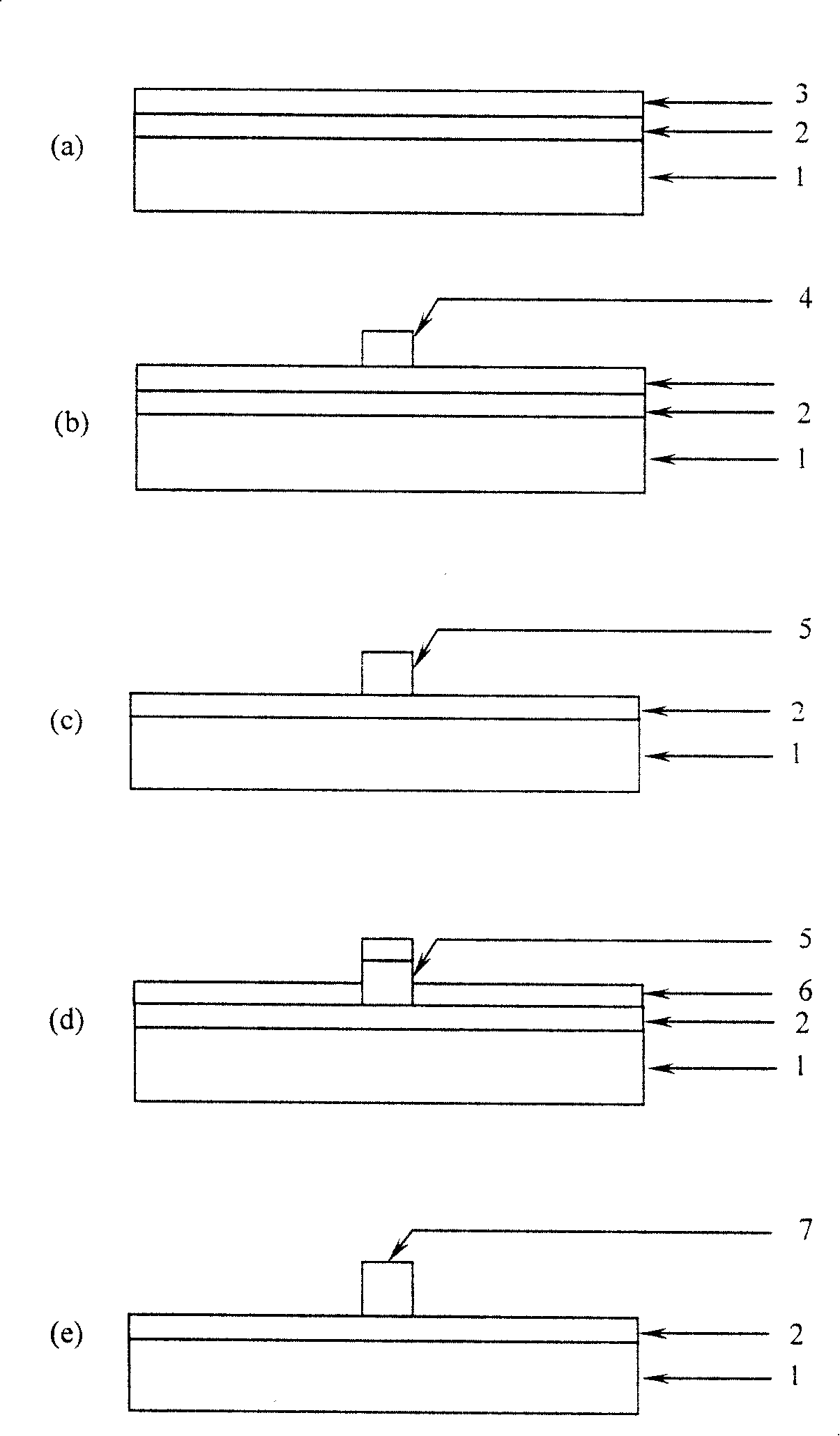
[0046] refer to figure 1 , make the nickel silicide nanostructure of this embodiment according to the flow process of the present invention:

[0047] 1) Select an SOI substrate with a thin layer of single crystal silicon prepared by oxygen injection isolation technology, and its crystal orientation is (100). The SOI substrate consists of an insulating dielectric interlayer 2 grown on a single crystal silicon wafer 1 and a top silicon Composed of thin film 3; the top silicon thin film 3 is monocrystalline silicon, its thickness is 100 nanometers, and the thickness of insulating medium interlayer 2 is 350 nanometers;

[0048] 2) After the SOI substrate described in step 1) is washed and dried with acetone, alcohol and deionized water, spin-coat the positive photoresist PMMA, and pre-bake it on a hot plate at 180 ° C for 1 minute. The thickness of the resist is about 100 nanometers, and the Raith 150 electron beam exposure system is used to directly write two rectangular pattern...

Embodiment 2

[0054] For the nickel silicide nanostructure prepared in this embodiment, see figure 2 , the width of the nickel silicide line shown in the figure is 280 nm.

[0055] refer to figure 1 , the preparation method of this example is according to figure 1 The technological process is carried out, and the detailed description is as follows:

[0056] 1) Spin-coat HSQ solution on a single crystal silicon substrate (single crystal silicon support layer 1), bake at 250°C for 2 minutes, and form an HSQ insulating dielectric interlayer 2 with a thickness of about 150 nanometers, and then use magnetron sputtering Thin layer of polysilicon is spray-deposited with a thickness of about 80 nanometers to form an SOI substrate

[0057] 2) Spin-coat the negative photoresist (SAL 601) on the SOI substrate prepared in step 1), and pre-bake it on a hot plate at 105°C for 2 minutes. The exposure system exposes a series of lines with a length of 100 microns and a width of 250 nanometers, post-bak...

Embodiment 3

[0063] refer to figure 1 , the technical process of making titanium disilicide nanostructure in this embodiment is according to figure 1 As shown, the specific steps are as follows:

[0064] 1) Select an SOI substrate with a thin single crystal silicon layer prepared by oxygen injection isolation technology, its crystal orientation is (100), the thickness of the top silicon layer is reduced to 50 nanometers after reactive ion etching, and the silicon oxide buried layer The thickness is 350 nm.

[0065] 2) Spin-coat the positive photoresist PMMA on the SOI substrate thinned in step 1), bake at 180°C for 1 minute, the thickness of the photoresist is about 100 nanometers, and put it into a Raith 150 electron beam exposure system for exposure. The pattern design is a square array with a side length of 4.9 micrometers and a period of 5.0 micrometers, which leaves mutually orthogonal lines with a width of about 100 nanometers after exposure. After developing and fixing, the phot...


PUM

PropertyMeasurementUnit
thicknessaaaaaaaaaa
thicknessaaaaaaaaaa
thicknessaaaaaaaaaa

Abstract

The invention relates to a material with metal silicide nanometer structure and the preparation method thereof. The material comprises a metal silicide nanometer structure which is produced on an SOI substrate; the thickness of an insulation medium layer of the SOI substrate is 100 to 1000 nanometers, and the thickness of silicon thin film is 50 to 500 nanometers. The preparation method comprises the following steps: a required mask feature structure of nanometer structure is produced on the silicon thin film surface of the SOI substrate after cleaning, drying, spin coating positive photoresist, exposing, developing, and fixing; the silicon thin film of the SOI substrate is etched to the required nanometer structure by adopting a reactive ion etching, the etching depth is equal to the thickness of the silicon thin film, a metal thin film which is required by the metal silicide is deposited on the isolation layer which contains the silicon nanometer structure, then high temperatures anneal is performed to ensure that soild phase reaction is reacted between the metal and the silicon, thus to generate the metal silicide, the unreacted metal is removed through chemical etch, and then the metal silicide nanometer structure is formed. The method is simple, and the position and the dimension of the nanometer structure can be controlled.

Description

technical field [0001] The invention relates to a metal silicide nanostructure and a manufacturing method thereof, in particular to being compatible with an integrated circuit manufacturing process, having a controllable shape and growth position, and having good applications in the fields of integrated circuits, microelectronic devices, and nanoelectronic devices. Prospect metal silicide nanostructures fabricated on SOI (silicon on insulator, thin silicon on insulating layer) substrates and their fabrication methods. Background technique [0002] Metal silicide has the characteristics of low resistivity, high thermal stability, good anti-electromigration performance and small mean free path of carriers, and has good application prospects in nanoelectronic devices and integrated circuits, such as As interconnect wires, source drain and gate electrodes, etc. Fabrication of nanoscale metal silicides is becoming more and more important as device sizes decrease. Taking nanowir...

Claims


Application Information

Patent Timeline
Patent Type & Authority Applications(China)
IPC IPC(8): H01L27/12H01L21/84H01L21/762H01L21/30H01L21/308
Inventor 罗强王强顾长志金爱子李俊杰杨海方
Owner INST OF PHYSICS - CHINESE ACAD OF SCI
Why Eureka
Try Eureka