Method for manufacturing erbium-doped hybrid SiO2 optical waveguides amplifier by ultraviolet light direct-writing

An optical waveguide amplifier and a technology for a waveguide amplifier, which are applied in the field of optical communication, can solve the problems of affecting the quality of the waveguide, complicated process, sticking and the like, and achieve the effects of cost saving, simple preparation process and low heat treatment temperature.

Inactive Publication Date: 2008-12-31
INST OF SEMICONDUCTORS - CHINESE ACAD OF SCI
View PDF0 Cites 6 Cited by
  • Summary
  • Abstract
  • Description
  • Claims
  • Application Information

AI Technical Summary

Problems solved by technology

However, the traditional sol-gel method is difficult to obtain SiO with a thickness that meets the device requirements and is free of cracks. 2 Thin film, multiple coating-annealing preparation process will cause spots, sticky dirt and other defects on the film, which will affect the quality of the waveguide and increase the loss of the device
[0004] The typical manufacturing process of existing optical waveguide amplifiers is: a series of processes such as pattern masking, photolithography, development and reactive ion etching are produced on the core layer. This process is complex, expensive equipment, high production cost, and low efficiency. , not suitable for large-scale mass production

Method used


Image

  • Method for manufacturing erbium-doped hybrid SiO2 optical waveguides amplifier by ultraviolet light direct-writing
  • Method for manufacturing erbium-doped hybrid SiO2 optical waveguides amplifier by ultraviolet light direct-writing
  • Method for manufacturing erbium-doped hybrid SiO2 optical waveguides amplifier by ultraviolet light direct-writing

Examples


Embodiment Construction

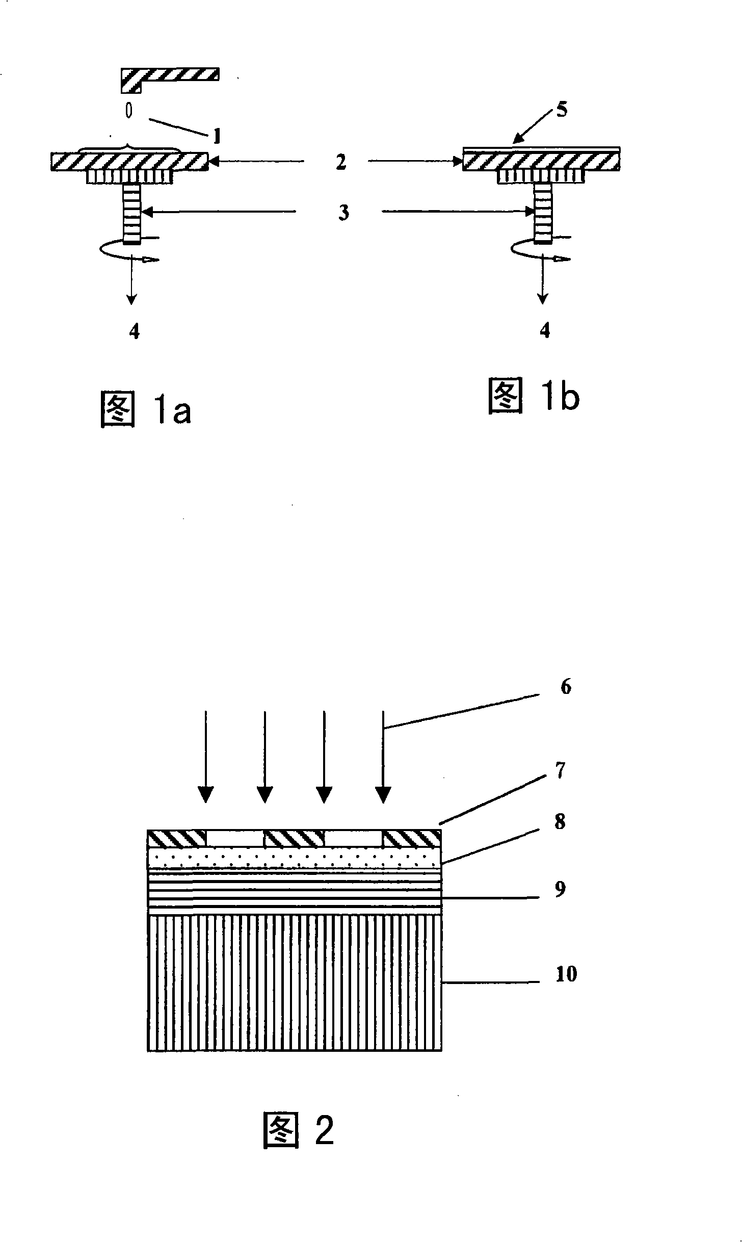
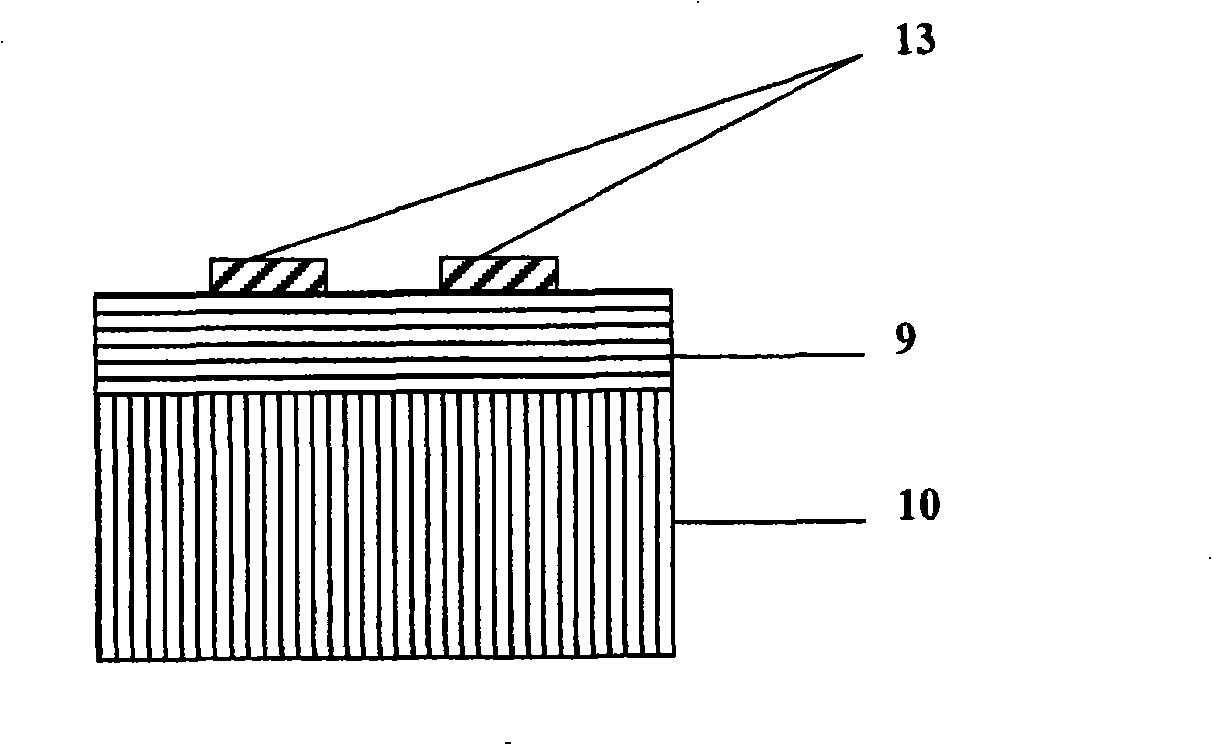
[0026] See Figure 2- Figure 4 Described, a kind of ultraviolet light direct writing of the present invention makes erbium-doped hybrid SiO 2 The method for optical waveguide amplifier, comprises the steps:

[0027] Step 1: first grow the lower cladding layer 9 on the single crystal Si substrate 10 by thermal oxidation method, the thickness of the lower cladding layer 9 is 10 microns-20 microns of SiO 2 ;

[0028] Step 2: Preparation of erbium-doped photosensitive SiO by organic / inorganic hybrid sol-gel method 2 material; the organic / inorganic hybrid erbium-doped photosensitive SiO 2 The preparation of the material is to use methacryloxypropyltrimethoxysilane as the reaction precursor, hydrochloric acid solution as the catalyst, mixing and stirring for hydrolysis, adding zirconium tetrapropoxide to adjust the refractive index, erbium nitrate solution to provide erbium ions, and positive Propanol is used as a solvent, and 1-hydroxy-cyclohexyl benzophenone is added to make t...


PUM

PropertyMeasurementUnit
refractive indexaaaaaaaaaa

Abstract

The invention provides a method used for preparing erbium-doped hybridization SiO2 optical waveguide amplifier by direct writing of ultraviolet. The method of the invention is characterized by comprising the steps as follows: step 1: a thermal oxidation method is used for generating a lower wrapping layer on a single-crystal Si underlay; step 2: an organic/inorganic hybridized sol-gel method is used to prepare the erbium-doped photosensitive SiO2 material; step 3: the photosensitive hybridized SiO2 film is rotatablely coated on the lower wrapping layer and taken as a core layer; step 4: front baking and solidifying operations are carried out; step 5: the exposure is carried out by using the ultraviolet to pass through a mask; device patterns are directly copied to the core layer; step 6: developing and rear baking operations are carried out so as to obtain the bar-shaped erbium-doped waveguide amplifier.

Description

technical field [0001] The invention belongs to a method for manufacturing an optical amplifier device in the technical field of optical communication, in particular to a method for making erbium-doped hybrid SiO by direct writing with ultraviolet light 2 The method of optical waveguide amplifier. Background technique [0002] Erbium-doped optical waveguide amplifier (EDWA), due to its internal erbium ion Er 3+ energy level 4 I 13 / 2 → 4 I 15 / 2 Stimulated transition can amplify optical signals in the communication wavelength range of 1.55 μm, and has a compact optical waveguide structure, small size, can be integrated, and is easy to realize photoelectric hybrid integration, so it has received extensive attention and research, and is used in The field of optical communication has good development prospects. [0003] At present, the production of erbium-doped optical waveguide amplifiers is to first grow SiO on Si substrates. 2 The lower cladding layer, and then use fla...

Claims


Application Information

Patent Timeline
Patent Type & Authority Applications(China)
IPC IPC(8): G02B6/13G03F7/00G02F1/39
Inventor 王鵫吴远大李建光王红杰安俊明胡雄伟
Owner INST OF SEMICONDUCTORS - CHINESE ACAD OF SCI
Why Eureka
Try Eureka