Method for preparing colorful film for protecting solar cell thin grid line metal electrode by adopting mask

A metal electrode, solar cell technology, applied in the field of solar cells, can solve problems such as restricting architects, unable to better meet people's aesthetic needs, monotonous color of solar cells, etc., to achieve good industrialization prospects, meet design diversity, Protects against oxidation

Inactive Publication Date: 2010-09-15
SUN YAT SEN UNIV
View PDF3 Cites 30 Cited by
  • Summary
  • Abstract
  • Description
  • Claims
  • Application Information

AI Technical Summary

Problems solved by technology

Today, with the increasingly close combination of solar cells and buildings, especially the growing development of building-integrated photovoltaics (BIPV), the monotonous color of solar cells restricts the inspiration of architectural designers and cannot better meet people's aesthetic needs.

Method used


Image

  • Method for preparing colorful film for protecting solar cell thin grid line metal electrode by adopting mask
  • Method for preparing colorful film for protecting solar cell thin grid line metal electrode by adopting mask
  • Method for preparing colorful film for protecting solar cell thin grid line metal electrode by adopting mask

Examples


Embodiment 1

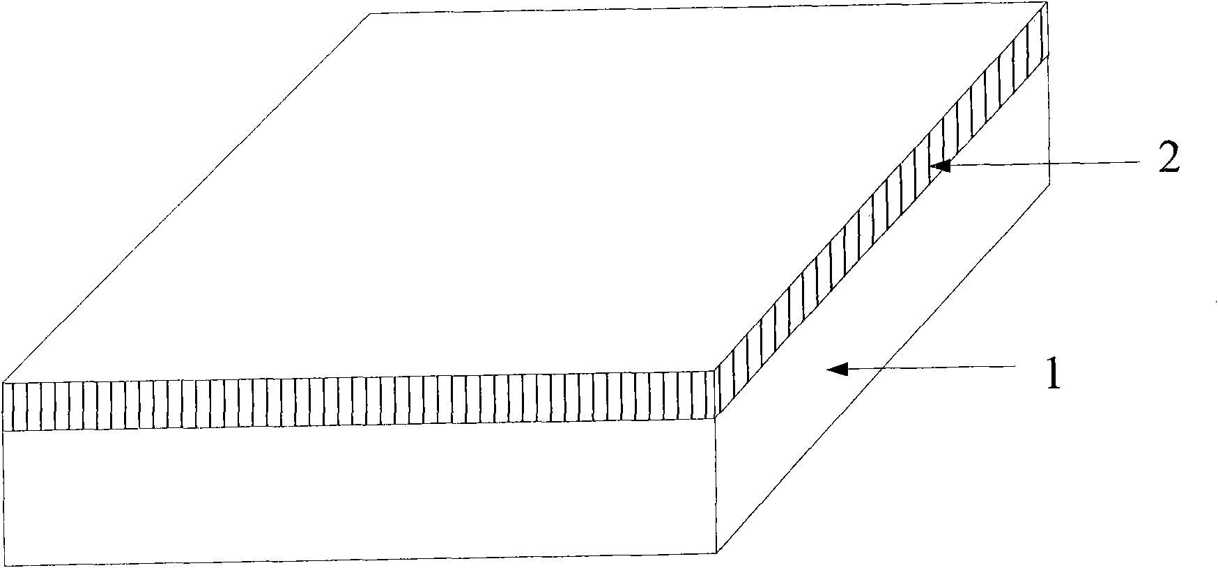
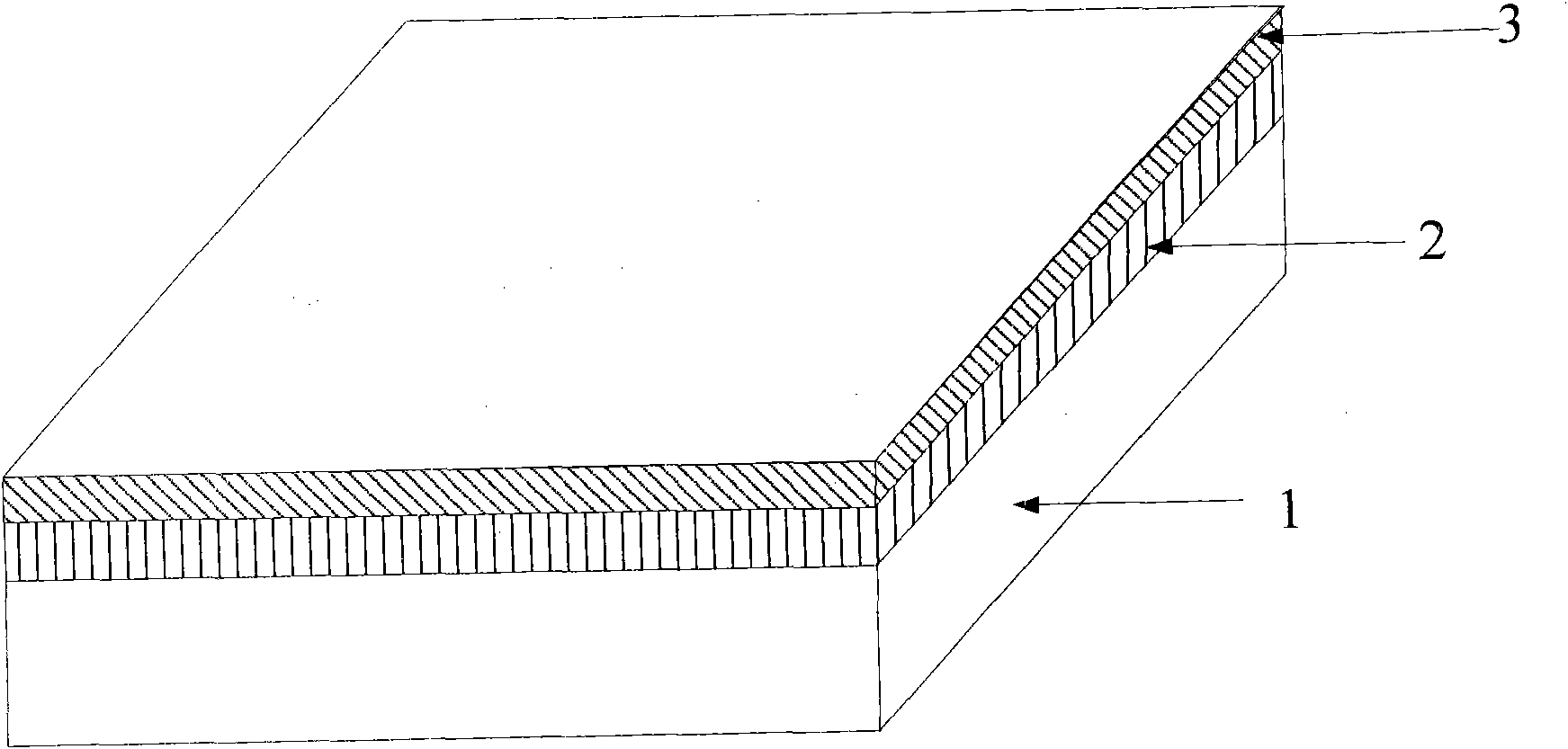
[0039] as attached Figure 1-3As shown, the p-type single crystal silicon wafer 1 is cleaned and acid-textured. Then, the phosphorous oxychloride gas is fed into the tubular diffusion furnace, and phosphorus is diffused at a high temperature of 800° C. to form a p-n junction 2 . Use 5% hydrofluoric acid aqueous solution to remove phosphosilicate glass, use plasma etching method to remove edges, and then use evaporation, sputtering, deposition, ion plating or CVD method, in this case, PECVD method is used , coating a layer of silicon nitride passivation film 3 with a thickness of 40nm and a refractive index of 2.1 above the n-type region. The passivation layer can also improve the passivation effect by increasing the hydrogen content, and at the same time reduce the thickness of the passivation layer to avoid Excessive absorption of light by a passivation layer. Use screen printing to print silver-aluminum paste on the back, dry it in a drying oven at a temperature zone of 18...

Embodiment 2

[0042] as attached Figure 1-3 As shown, the p-type silicon wafer 1 is cleaned and alkali-textured. Then, the phosphorous oxychloride gas is fed into the tubular diffusion furnace, and phosphorus is diffused at a high temperature of 800° C. to form a p-n junction 2 . Use 5% hydrofluoric acid aqueous solution to remove phosphosilicate glass, use plasma etching to remove edges, and then use PECVD to plate a composite passivation film 3 of silicon oxide and silicon nitride on the n-type region, wherein , the refractive index of silicon oxide is 1.46, and the thickness is 30nm; the refractive index of silicon nitride is 2.1, and the thickness is 20nm. Use screen printing to print silver-aluminum paste on the back, dry it in a drying oven at a temperature zone of 180-260°C, then print aluminum paste, and dry it again; The temperature zone is sintered to form the aluminum back field, the silver-aluminum electrode 4 and the front surface electrode, the fine-grid silver electrode 5 ...

Embodiment 3

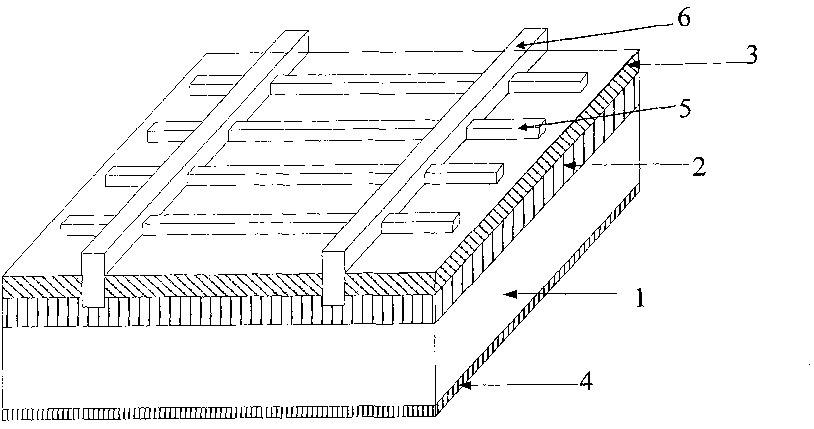
[0045] as attached Figure 1-3 As shown, the n-type polysilicon wafer 1 is cleaned and acid-textured. Boron diffusion is then performed to form a p-n junction 2 . Wash with 5% hydrofluoric acid aqueous solution, then use plasma etching to remove edges, and use PECVD to coat an amorphous silicon passivation film with a thickness of 20nm and a refractive index of 2.0 on the n-type region 3. Use the screen printing method to print silver and aluminum paste on the back, dry it in a drying oven at a temperature zone of 180-260°C, then print aluminum paste, and dry it again; print silver paste on the front, and dry it at a temperature of 200-860°C The area is sintered to form aluminum back field, silver-aluminum electrode 4 and front surface electrode fine-grid silver electrode 5 and busbar silver electrode 6. The width of the formed busbar metal electrode is 3mm, and the width of the fine-grid metal electrode is 120 μm. as attached Figure 4-7 As shown, prepare a metal mask mo...


PUM

PropertyMeasurementUnit
widthaaaaaaaaaa
widthaaaaaaaaaa
thicknessaaaaaaaaaa

Abstract

The invention relates to a method for preparing a colorful film for protecting a solar cell thin grid line metal electrode by adopting a mask. In the method, after a solar cell is prepared, a mask is utilized to cover a main grid line metal electrode on the front surface of the solar cell, a film is coated on the area which is not covered by the mask for the second time, and a dielectric layer for protecting the thin grid line metal electrode is prepared to form a structure comprising the dielectric layer, the thin grid line metal electrode and a passivation layer. The method can protect the thin grid line metal electrode against easy oxidation, and the main grid line metal electrode can be normally connected by welding rods. The passivation effect of the front surface can be enhanced through optimizing the passivation layer; the reflectivity of the front surface of the solar cell can be reduced and color regulation can be realized through regulating the dielectric layer; and characters, figures, graphics and the like can be displayed on the front surface of the solar cell through changing a mask pattern. In addition, the secondary film coating method is convenient to be in butt joint with the traditional crystalline silicon solar cell preparation process and is easy for industrialization.

Description

technical field [0001] The invention belongs to the technical field of solar cells, and in particular relates to a method for preparing a color thin film for protecting fine grid line metal electrodes of solar cells by using a mask. Background technique [0002] At present, the conventional process for preparing crystalline silicon solar cells generally uses PECVD to plate a single layer of silicon nitride (SiN) on the front surface of crystalline silicon solar cells. x ), and then print a layer of silver paste on the silicon nitride by screen printing, make the silver paste burn through the silicon nitride by sintering, and form an ohmic contact with silicon to prepare the front electrode. Since the metal grid is located on the top layer of the solar cell and is in direct contact with the air, during the transportation of the battery from the battery manufacturer to the component manufacturer, the front silver electrode metal grid may be oxidized by oxygen in the air due to...

Claims


Application Information

Patent Timeline
Patent Type & Authority Applications(China)
IPC IPC(8): H01L31/18
CPCY02P70/50
Inventor 沈辉陈奕峰许欣翔梁学勤
Owner SUN YAT SEN UNIV
Why Eureka
Try Eureka