A gradient doped silicon-based heterojunction solar cell and its preparation method

A solar cell and gradient doping technology, which is applied in the field of solar cells, can solve the problems that cannot be pushed to the pn junction region to increase the photocurrent, achieve high photoelectric conversion efficiency, increase short-circuit current, and reduce losses

Inactive Publication Date: 2011-12-14
SHANGHAI NORMAL UNIVERSITY
View PDF3 Cites 24 Cited by
  • Summary
  • Abstract
  • Description
  • Claims
  • Application Information

AI Technical Summary

Problems solved by technology

There is no built-in electric field in a uniformly doped semiconductor, so the minority carriers in the thin film layer cannot be effectively pushed to the pn junction region to increase the photocurrent

Method used


Image

  • A gradient doped silicon-based heterojunction solar cell and its preparation method
  • A gradient doped silicon-based heterojunction solar cell and its preparation method
  • A gradient doped silicon-based heterojunction solar cell and its preparation method

Examples


Embodiment 1

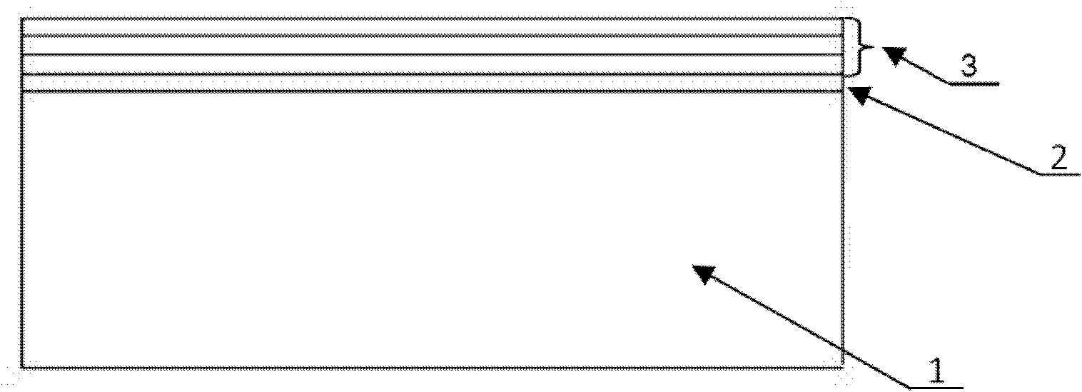
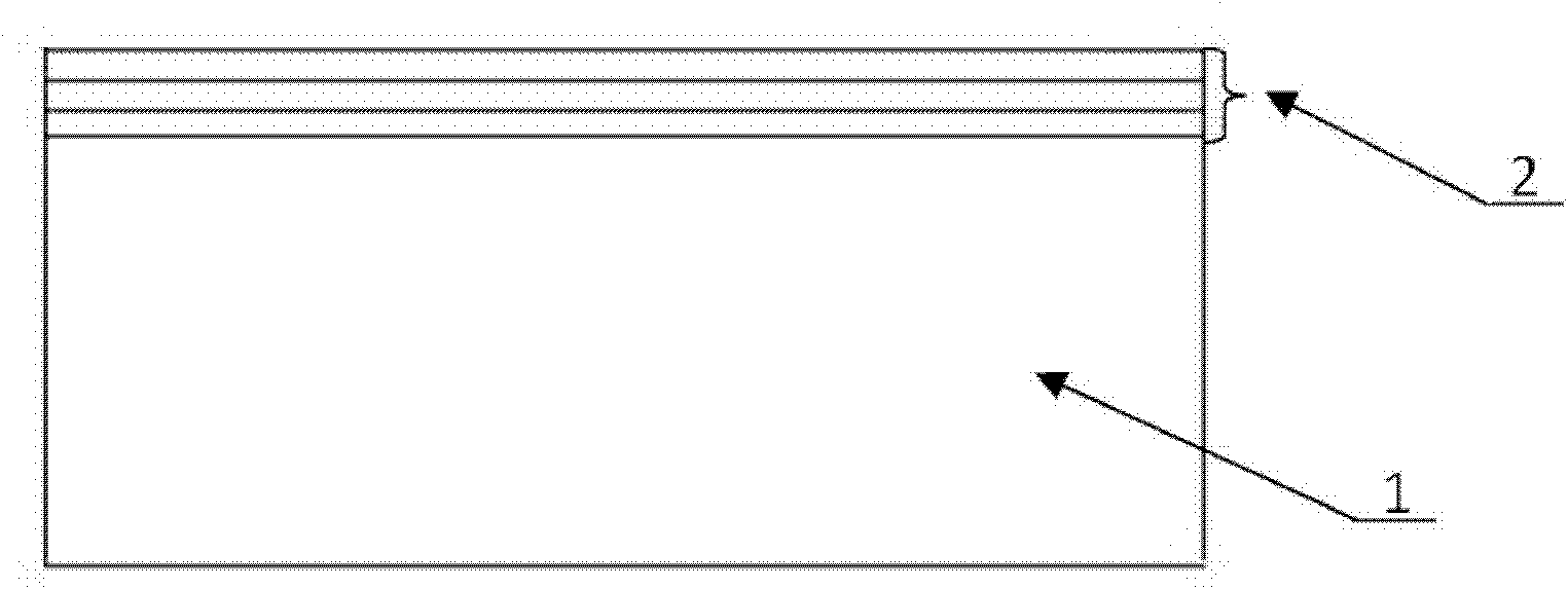
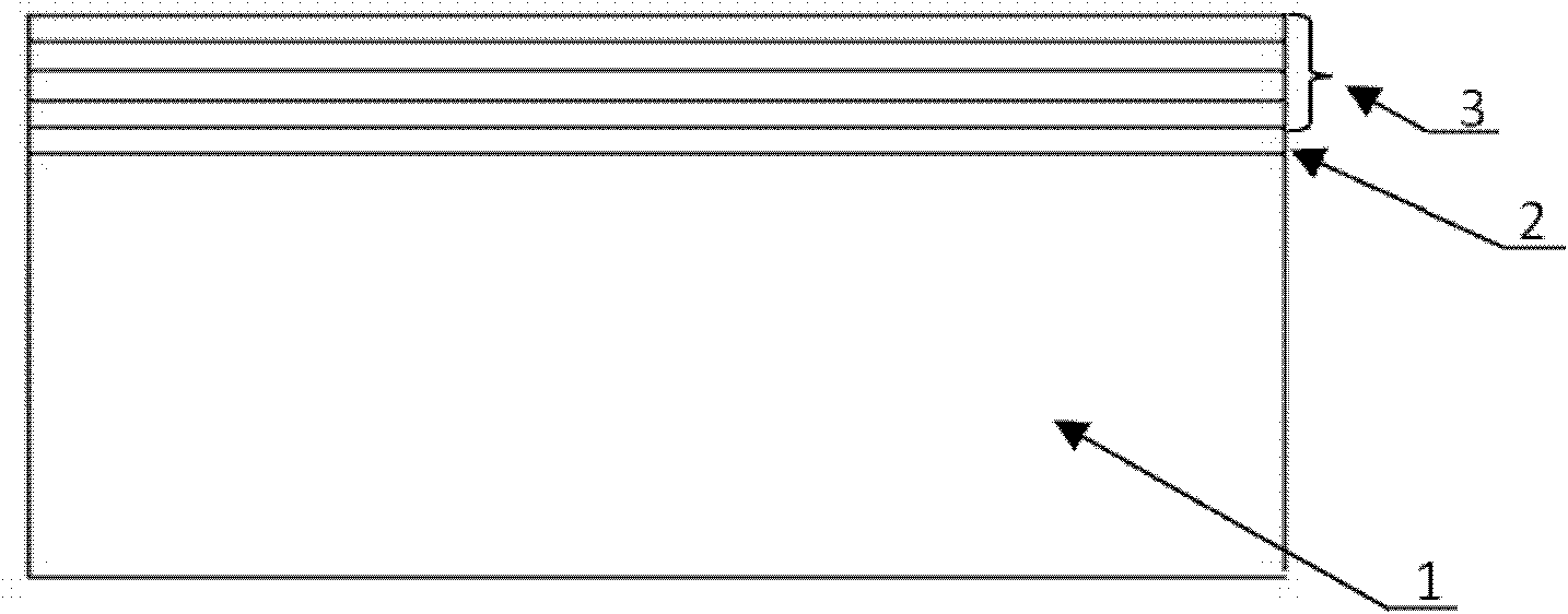
[0030](1) In this embodiment, a p-type single crystal silicon substrate Ω·cm with a resistivity of 3Ω·cm produced by zone melting is adopted, the orientation of the single crystal silicon is (100), and the thickness is 300 μm. First measure 300mL of deionized water, 300mL of ethanol and 300mL of acetone into the container to make a 1:1:1 mixed cleaning solution, and then put such figure 1 Put the single crystal silicon substrate 1 shown in the mixed cleaning solution, put the container containing the mixed cleaning solution and the substrate into an ultrasonic cleaner, and perform ultrasonic cleaning for 15 minutes. After cleaning, put the substrate into an oven to dry Drying, the oven temperature is set to 130 ° C; then the mixed solution of hydrochloric acid and hydrogen peroxide prepared according to the volume ratio of 1:1 is used to remove the metal impurities on the surface of the single crystal silicon substrate, washed with deionized water and then dried;

[0031] (2) ...

Embodiment 2

[0046] (1) The p-type monocrystalline silicon chip of resistivity 3Ω cm produced by zone melting is used as substrate, and all the other are with embodiment 1 step (1);

[0047] (2) same as step (2) in embodiment 1;

[0048] (3) same as step (3) in embodiment 1;

[0049] (4) same as step (4) in embodiment 1;

[0050] (5) Put the dried p-type single crystal silicon substrate above into the PECVD deposition chamber, and evacuate the body to 1×10 -5 Pa, the substrate temperature is heated to 185° C., and then hydrogen, silane, and phosphine gas diluted with hydrogen are introduced as reaction gases. The volume content of phosphine in the phosphine gas used is 5%, and the rest is hydrogen. The doping concentration in the doped amorphous silicon film is controlled by controlling the flow of phosphine gas, and the total flow of silane, hydrogen, and phosphine gas is controlled to be 100 sccm. First, the flow rate of silane is 5 sccm, the flow rate of hydrogen gas is 94.5 sccm, th...

Embodiment 3

[0062] (1) The n-type monocrystalline silicon chip of resistivity 3Ω cm produced by zone melting is used as substrate, and all the other are with embodiment 1 step (1);

[0063] (2) same as step (2) in embodiment 1;

[0064] (3) same as step (3) in embodiment 1;

[0065] (4) same as step (4) in embodiment 1;

[0066] (5) Put the dried n-type single crystal silicon substrate into the PECVD deposition chamber, and evacuate to 1×10 -5 Pa, the substrate temperature is heated to 200°C, then feed hydrogen and silane as reaction gas, the flow of hydrogen is 95 sccm, the flow of silane is 5 sccm, the total flow is 100 sccm, that is, the volume concentration of silane in the reaction gas is 5%, The pressure of the PECVD deposition chamber was controlled at 50 Pa. After the state was stabilized, the RF power was turned on and the power was adjusted to 50 W. The deposition was performed for 2 minutes, and then the RF power was turned off to stop the deposition. At this point the depos...


PUM

PropertyMeasurementUnit
thicknessaaaaaaaaaa
thicknessaaaaaaaaaa
thicknessaaaaaaaaaa

Abstract

The invention discloses a gradient doped silicon-based heterojunction solar cell and a preparation method thereof. A plurality of layers of amorphous silicon membranes of which the doped concentration is increased sequentially are deposited on the surface of crystalline silicon serving as a substrate, and a transparent conductive film with a certain thickness is deposited and an electrode is prepared to prepare the gradient doped silicon-based heterojunction solar cell, wherein the amorphous silicon membranes contact the crystalline silicon to achieve a good passivating effect and obtain highopen-circuit voltage; a plurality of gradient doped amorphous silicon layers can form a strong inner electric field to reduce the composite loss of photo-induced carriers, improve the collection rateof minority carriers and increase short-circuit current; and the doped concentration of the doped amorphous silicon layers contacting the electrode is high, the resistivity is low, and contact resistance between the doped amorphous silicon layers and the electrode can be reduced to improve filling factors of the solar cell. Therefore compared with the conventional silicon-based heterojunction solar cell, the gradient doped silicon-based heterojunction solar cell has high photoelectric conversion efficiency.

Description

technical field [0001] The invention relates to the technical field of solar cells, and relates to a gradient doped silicon-based heterojunction solar cell and a preparation method thereof. Background technique [0002] With the continuous progress and improvement of human civilization and living standards, human demand for energy is increasing. However, the primary energy resources (such as oil, coal, natural gas, nuclear fuel, etc.) on the earth are becoming less and less, and eventually will dry up. At the same time, the consumption of disposable energy is also accompanied by huge environmental pollution and a large amount of greenhouse gas emissions, which directly threaten the sustainable development of human society. Therefore, the development of renewable and clean energy technologies is the key to the sustainable development of human society. one. Solar cells can directly convert inexhaustible and inexhaustible sunlight into electrical energy, which is a clean and ...

Claims


Application Information

Patent Timeline
Patent Type & Authority Applications(China)
IPC IPC(8): H01L31/0352H01L31/072H01L31/20
CPCY02E10/50Y02P70/50
Inventor 杜国平齐立敏
Owner SHANGHAI NORMAL UNIVERSITY
Why Eureka
Try Eureka