Method for testing content of metal ions on surface of 8-inch silicon polished wafer for insulated gate bipolar transistor (IGBT)

A technology for surface metal and ion content, applied in measuring devices, material analysis through electromagnetic means, instruments, etc., can solve the problems of low light metal elements, not widely used, complicated quantitative calibration operations, etc., and achieve stable recovery rate , reduce the possibility, improve the effect of test accuracy

Inactive Publication Date: 2012-07-11
TIANJIN ZHONGHUAN ADVANCED MATERIAL TECH
View PDF2 Cites 7 Cited by
  • Summary
  • Abstract
  • Description
  • Claims
  • Application Information

AI Technical Summary

Problems solved by technology

[0004] At present, manual VPD is mostly used in China for pre-processing and most of the silicon wafers are 6 inches or smaller in size. That is, the operator uses a vacuum suction pen to suck the back of the silicon wafer, drops a drop of scanning liquid on the front of the silicon wafer, and tilts the silicon wafer to make the scanning liquid After scanning the entire silicon wafer, use a liquid pick-up gun to suck the scanning liquid into the ICPMS for testing. In this way, impurities will inevitably be introduced during the test process, which will affect the test effect. Since the surface area of ​​the 8-inch silicon wafer is larger, its manual VPD process is compared with 6-inch silicon wafers are more likely to introduce metal ions in the environment, personnel and operation process; in addition, manual VPD cannot scan the entire silicon wafer to the same extent, so ideal test results cannot be obtained
[0005] On the other hand, for the test method, TXRF uses X-rays as the excitation source of fluorescence, so the response to light metal elements (such as Na, Mg, Al) is too low, making ultra-trace detection impossible
TOS-SIMS can detect all elements, but it is not widely used because of its complicated operation in quantitative calibration

Method used


Image

  • Method for testing content of metal ions on surface of 8-inch silicon polished wafer for insulated gate bipolar transistor (IGBT)
  • Method for testing content of metal ions on surface of 8-inch silicon polished wafer for insulated gate bipolar transistor (IGBT)
  • Method for testing content of metal ions on surface of 8-inch silicon polished wafer for insulated gate bipolar transistor (IGBT)

Examples


Embodiment Construction

[0035] In order to understand the present invention more clearly, describe the present invention in detail in conjunction with accompanying drawing and embodiment:

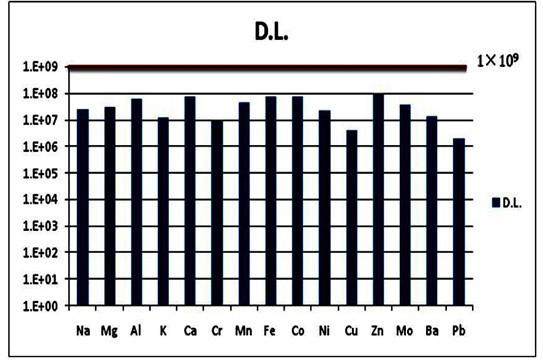
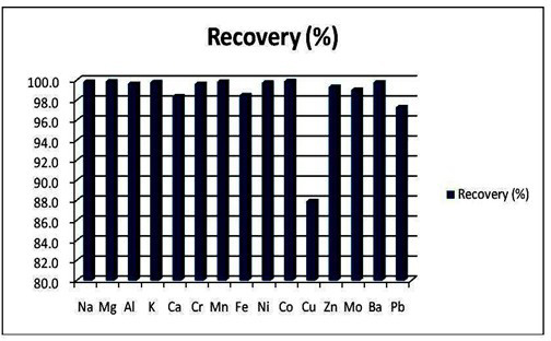
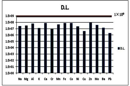
[0036] The invention utilizes full-automatic VPD pretreatment and ICPMS (inductively coupled plasma mass spectrometer) to realize the test of ultra-trace metal ion content on the surface of an 8-inch silicon single crystal polished wafer. Concrete preparation process is as follows:

[0037] 1) The test object used in the experiment is: 8-inch silicon polished wafer, diameter 200mm, thickness 440μm, doped with P crystal orientation, resistivity 5-10Ω; use ADE CR81e to scan after cleaning with SC-1 and SC-2 Particles (0.3um<10), no defects on the surface.

[0038] 2) The reagent specifications used in the experiment are: hydrogen peroxide (H2O2): 35±1%, TAMA AA-10 grade, hydrofluoric acid (HF): 38%, TAMA AA-10 grade; nitric acid (HNO3): 68%, TAMA AA-100 grade; ultrapure water: resistivity ≥ 18M Ω cm, Mill...


PUM

PropertyMeasurementUnit
electrical resistivityaaaaaaaaaa
diameteraaaaaaaaaa
thicknessaaaaaaaaaa

Abstract

The invention relates to a method for testing the content of metal ions on the surface of an 8-inch silicon polished wafer for an insulated gate bipolar transistor (IGBT). By using fully-automatic vapor phase decomposition (VPD) pretreatment equipment which is manufactured by a Korea Expert company and an Agilent-7700 inductively coupled plasma mass spectrometer of an Agilent company, the content of ultra-trace metal including sodium (Na), magnesium (Mg), aluminum (Al), potassium (K), calcium (Ca), chromium (Cr), manganese (Mn), iron (Fe), cobalt (Co), nickel (Ni), copper (Cu), zinc (Zn), molybdenum (Mo), barium (Ba) and lead (Pb) on the surface of the 8-inch silicon polished wafer is detected. Compared with the conventional manual VPD method, the method provided by the invention has the advantages that: the probability of introduction of external metal irons can be greatly reduced by using a fully-automatic VPD system; recovery rate is stabilized; testing accuracy is improved; full-element and ultra-trace detection of an 8-inch monocrystalline silicon polished wafer is realized; a detection limit is lower than 1*10<9>atom / cm<2>; and the recovery rate of a great majority of elements is over 96 percent.

Description

technical field [0001] The invention relates to the technical field of detection of semiconductor silicon polished wafers, in particular to a method for testing the metal ion content on the surface of an 8-inch silicon polished wafer for IGBT. Background technique [0002] At present, the semiconductor manufacturing industry is gradually developing towards high operating speed and smaller device size. The size of semiconductor devices continues to shrink, the density of components in chips continues to increase, and the distance between components becomes smaller and smaller, even down to the nanometer level. However, trace impurity elements introduced between components during the entire production process may reduce the yield of chips. Specific pollution problems can lead to different defects in semiconductor devices, such as alkali metal and alkaline earth metal (Na, K, Ca, Mg, Ba, etc.) pollution can lead to a decrease in the breakdown voltage of the device; tra...

Claims


Application Information

Patent Timeline
Patent Type & Authority Applications(China)
IPC IPC(8): G01N27/64
Inventor 吴晓明吕莹王国瑞张晋英
Owner TIANJIN ZHONGHUAN ADVANCED MATERIAL TECH
Why Eureka
Try Eureka