

Structure using graphite alkene as buffer layer epitaxy GaN (gallium nitride) and preparation method of structure
A technology of graphene layer and buffer layer, which is applied in the field of optoelectronics, can solve the problems of inability to alleviate the stress and thermal expansion coefficient mismatch between the substrate and the epitaxial material, reduce the quality of sapphire and gallium nitride, and reduce the quality of the epitaxial crystal, etc., so as to reduce the leakage current , Mitigation of thermal expansion coefficient mismatch, low stress effect
- Summary
- Abstract
- Description
- Claims
- Application Information
AI Technical Summary
Problems solved by technology
Method used
Image

Examples
Embodiment 1
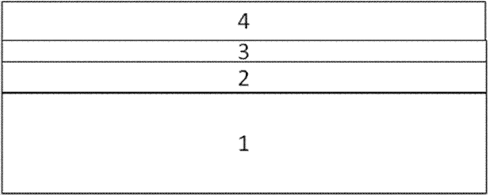
[0036] An epitaxial GaN structure using graphene as a buffer layer, including a silicon carbide substrate 1, a graphene layer 2 and a GaN layer 4; a thin aluminum gallium nitride layer 3 is arranged between the graphene layer 2 and the GaN layer 4; On the silicon carbide substrate 1 are a graphene layer 2, an aluminum gallium nitride thin layer 3, and a GaN layer in sequence. The thickness of the silicon carbide substrate 1 is 600 μm; the thickness of the graphene layer is 10 nm, and the number of layers is 30; the thickness of the GaN layer 4 is 6 μm: the thickness of the aluminum gallium nitride thin layer 3 is 100nm.
Embodiment 2
[0038] A method for preparing the structure described in Example 1, the steps are as follows:
[0039] 1) Clean the silicon carbide substrate, prepare the graphene layer on the substrate by physical vapor deposition, and put the substrate into a high-vacuum high-frequency heating furnace. The thickness of the silicon carbide substrate is 600μm, and the temperature is heated Graphene is grown according to the prior art at 1500°C, and the thickness of the graphene layer is 10nm;
[0040] 2) A thin layer of aluminum gallium nitride 3 is grown on the graphene layer formed in step 1), the thickness of the thin aluminum gallium nitrogen layer 3 is 100 nm, the growth temperature is 900° C., and the growth rate range is 30 nm / min, The carrier gas used is a mixture of nitrogen and hydrogen at a volume ratio of 1:1;
[0041] 3) The GaN layer 4 is grown on the aluminum gallium nitrogen thin layer 3 by metal organic chemical vapor deposition, the growth rate is 2 μm / h, the growth temperature is...
Embodiment 3
[0044] An epitaxial GaN structure using graphene as a buffer layer, comprising a silicon carbide substrate 1, a graphene layer 2 and a GaN layer 4; a thin layer of indium gallium nitride 3 is arranged between the graphene layer 2 and the GaN layer 4; On the silicon carbide substrate 1 are a graphene layer 2, an indium gallium nitride thin layer 3, and a GaN layer in sequence. The thickness of the silicon carbide substrate 1 is 500 μm; the thickness of the graphene layer is 10 nm; the thickness of the GaN layer 4 is 8 μm; the thickness of the indium gallium nitride thin layer 3 is 150 nm.
PUM
| Property | Measurement | Unit |
|---|---|---|
| thickness | aaaaa | aaaaa |
| thickness | aaaaa | aaaaa |
| thickness | aaaaa | aaaaa |
Abstract
Description
Claims
Application Information