Oxide semiconductor film and preparation method thereof, thin film transistor and preparation method
An oxide semiconductor and oxide technology, which is applied in the manufacture of semiconductor/solid-state devices, semiconductor devices, and devices that coat surfaces with liquids, and can solve problems such as low carrier mobility and unsatisfactory performance of thin-film transistors.
- Summary
- Abstract
- Description
- Claims
- Application Information
AI Technical Summary
Problems solved by technology
Method used
Image

Examples
Embodiment 1
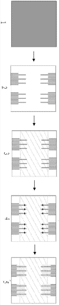
[0129] Embodiment 1, the preparation of zinc tin oxide thin film and its transistor and zinc tin oxide semiconductor thin film
[0130] Zinc tin oxide thin film has the advantages of rich and easily available raw materials, high transparency (with a band gap of 3.1 to 3.4eV), and good carrier transport performance.
[0131] The method for preparing zinc tin oxide semiconductor thin film with spin coating method is as follows:
[0132] (1) Preparation of precursor solution: Take Zn and Sn precursor materials zinc acetate and stannous chloride with a molar ratio of 1:1, add stabilizer ethylene glycol, dissolve in ethylene glycol monomethyl ether solvent, and stir well , until the solution is completely clarified, it generally takes 2 to 10 hours, and it is stirred for 4 hours in this embodiment. Set aside.
[0133] (2) Preparation of reaction solution: Before preparing the film, add a certain amount of water as a catalyst, stir until the solution is clarified to obtain a reactio...
Embodiment 2
[0149] Embodiment 2, the preparation of zinc tin oxide thin film and its transistor and zinc tin oxide semiconductor thin film
[0150] In this example, the zinc precursor used is zinc chloride, the tin precursor is tin tetraisopropoxide, the stabilizer is diethanolamine, the catalyst is ammonia water, the solvent is butanediol monomethyl ether, and other experimental conditions are the same as in the example 1. The molar ratio of zinc chloride, tin tetraisopropoxide, diethanolamine, and ammonia water is 0.3:0.3:2.0:1.5.
[0151] The 35nm thick zinc-tin oxide thin film prepared in the present embodiment measures its morphology (AFM figure, side length is 5 microns), such as Figure 8 . The zinc tin oxide thin film is very dense and flat, almost without any pinholes or crystal defects. The characterization parameters are as follows:
[0152] Scanning area: 5μm×5μm
[0153] Film valley value (P-V value) is 2.50nm
[0154] The root mean square roughness value (RMS value) is ...
Embodiment 3
[0156] Embodiment 3, the preparation of zinc tin oxide thin film and its transistor and zinc tin oxide semiconductor thin film
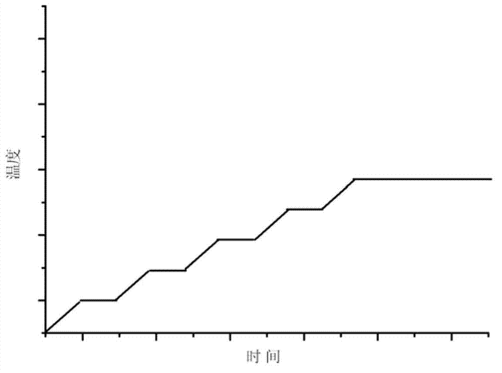
[0157] In this example, the heat treatment method adopted is to raise the temperature to 450° C. at a heating rate of 20° C. / min, and then treat at a constant temperature for 30 minutes. Other experimental conditions are the same as in Example 1.
[0158] The 30nm thick zinc-tin oxide thin film prepared in the present embodiment measures its morphology (AFM figure, side length is 5 microns), such as Figure 11 . The zinc tin oxide thin film has rough appearance and crystallization phenomenon. The characterization parameters are as follows:
[0159] Scanning area: 5μm×5μm
[0160] Film valley value (P-V value) is 95.9nm
[0161] The root mean square roughness value (RMS value) is 14.9nm
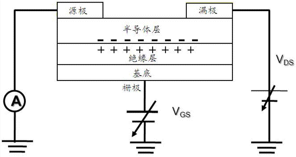
[0162] Using aluminum oxide thin film with a dielectric constant of 7.7 as the gate dielectric layer, an oxide thin film field effect transistor with zinc tin o...
PUM
| Property | Measurement | Unit |
|---|---|---|
| Carrier mobility | aaaaa | aaaaa |
| Carrier mobility | aaaaa | aaaaa |
| Carrier mobility | aaaaa | aaaaa |
Abstract
Description
Claims
Application Information
 - R&D
- Intellectual Property
- Life Sciences
- Materials
- Tech Scout
- Unparalleled Data Quality
- Higher Quality Content
- 60% Fewer Hallucinations
Browse by: Latest US Patents, China's latest patents, Technical Efficacy Thesaurus, Application Domain, Technology Topic, Popular Technical Reports.
© 2025 PatSnap. All rights reserved.Legal|Privacy policy|Modern Slavery Act Transparency Statement|Sitemap|About US| Contact US: help@patsnap.com