Flexible tubular microelectrode and preparation method thereof
A micro-electrode and tubular technology, applied in the field of micro-electrode and its preparation, can solve the problems of unsuitable use of rigid nerve electrodes, complicated manufacturing process, and high cost of electrode production, so as to facilitate processing and integration of implantable medical equipment and low cost , less prone to tissue damage
- Summary
- Abstract
- Description
- Claims
- Application Information
AI Technical Summary
Problems solved by technology
Method used
Image
Examples
Embodiment 1
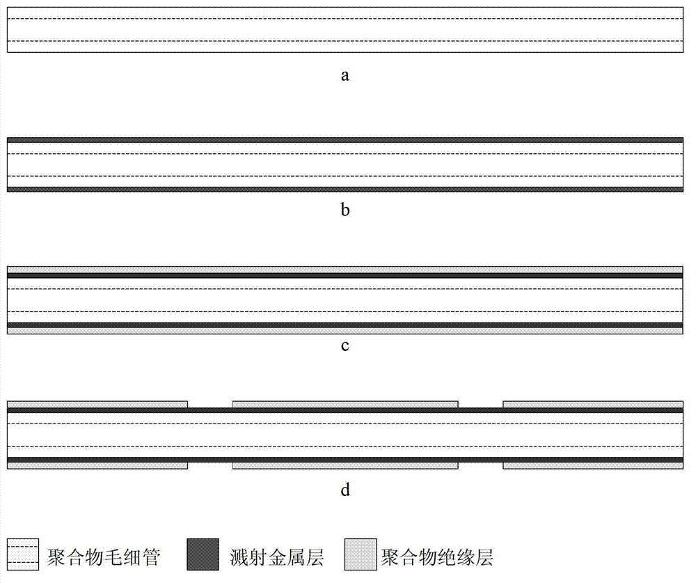
[0024] Such as figure 1 Shown, the present embodiment is prepared according to the following steps:
[0025] 1. Cut off a polyimide capillary with an outer diameter of 0.1 mm and clean it with ultrasonic vibration in deionized water;
[0026] 2. Sputter a titanium / tungsten / gold layer of 100-200 nanometers on the surface of the capillary, of which 30 nanometers of the titanium / tungsten layer is the bonding layer;
[0027] 3. Chemical vapor deposition of a parylene insulating layer of 3 to 10 microns on the capillary surface of the sputtered metal layer;
[0028] 4. Use a laser with a wavelength of 266 nm to etch away the surface insulating layer at a specific part of the capillary, with an etching width of 10-100 microns, to expose the electrode point of the metal layer, and obtain a polyimide tube gold microelectrode with an electrode point.
Embodiment 2
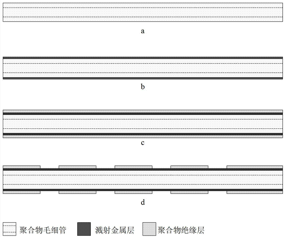
[0030] Such as figure 2 Shown, the present embodiment is prepared according to the following steps:
[0031] 1. Cut off a polyimide capillary with an outer diameter of 0.3 mm and clean it with ultrasonic vibration in deionized water;
[0032] 2. Sputtering a titanium / tungsten / platinum layer of 100-200 nanometers on the surface of the capillary, of which 30 nanometers of the titanium / tungsten layer is the bonding layer;
[0033] 3. Coating a polyimide insulating layer of 3 to 10 microns on the capillary surface of the sputtered metal layer;
[0034] 4. Use a laser with a wavelength of 266 nanometers to etch away the surface insulating layer at two specific parts of the capillary, with an etching width of 10-100 microns, to expose the metal layer electrode points, and obtain a polyimide tube platinum microelectrode with two electrode points.
Embodiment 3
[0036] Such as image 3 Shown, the present embodiment is prepared according to the following steps:
[0037] 1. Cut off a polytetrafluoroethylene capillary with an outer diameter of 0.3 mm and clean it with ultrasonic vibration in deionized water;
[0038] 2. Sputtering a titanium / tungsten / platinum layer of 100-200 nanometers on the surface of the capillary, of which 30 nanometers of the titanium / tungsten layer is the bonding layer;
[0039] 3. Chemical vapor deposition of a parylene insulating layer of 3 to 10 microns on the capillary surface of the sputtered metal layer;
[0040] 4. Using a laser with a wavelength of 266 nanometers to etch away the surface insulating layer at four specific parts of the capillary, the etching width is 10-100 microns, exposing the electrode points of the metal layer, and obtaining platinum microelectrodes of PTFE tubes with four electrode points.
[0041] It should be understood that the above are some embodiments of the present inventio...
PUM
| Property | Measurement | Unit |
|---|---|---|
| thickness | aaaaa | aaaaa |
| wavelength | aaaaa | aaaaa |
| width | aaaaa | aaaaa |
Abstract
Description
Claims
Application Information


