

Compound base of precious metal nanometer array and single layer graphene and preparation method thereof
A single-layer graphene and nanoarray technology, applied in the field of nanomaterials, can solve the problems of difficulty in obtaining large-area composite materials, reduced graphene performance, poor controllability, etc. less demanding effects
- Summary
- Abstract
- Description
- Claims
- Application Information
AI Technical Summary
Problems solved by technology
Method used
Image

Examples
Embodiment 1
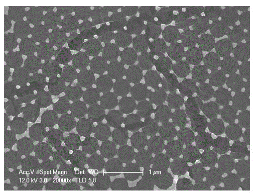
[0046]On a single-sided finely polished single-crystal silicon wafer, polystyrene nanospheres with a diameter of 460 nm were prepared by a liquid surface self-assembly method to form a single-layer closely arranged mask. Using a vacuum coating machine, a 10 nm thick Cr film was first evaporated on a polystyrene nanosphere mask, and then a 60 nm thick Ag film was evaporated to obtain a substrate. The substrate was sonicated in chloroform for 20 seconds and allowed to stand for 10 minutes to remove the polystyrene microspheres to obtain Ag nanoarrays, which were then washed in alcohol and deionized water in sequence.
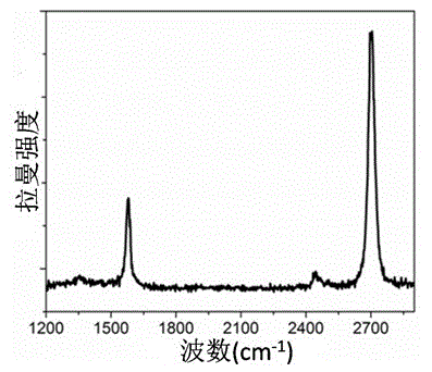
[0047] The Cu foil with a thickness of 25 μm was treated by chemical mechanical polishing to ensure that the surface of the Cu foil was clean and smooth; then, at 1020 ° C, in a mixed gas atmosphere of methane and hydrogen, the treated Cu foil was grown on the treated Cu foil by chemical vapor deposition. layer graphene, during the graphene growth process, the flo...
Embodiment 2
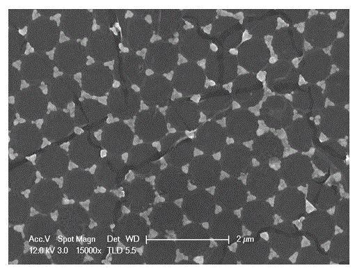
[0051] On a single-sided finely polished single-crystal silicon wafer, polystyrene nanospheres with a diameter of 800 nm were prepared by liquid surface self-assembly method to form a single-layer closely arranged mask. Using a vacuum coating machine, a 10 nm thick Cr film was first evaporated on a polystyrene nanosphere mask, and then a 60 nm thick Ag film was evaporated to obtain a substrate. Sonicate the substrate in chloroform for 20 seconds, let it stand for 10 minutes, remove the polystyrene nanosphere mask, and clean it in alcohol and deionized water in turn.
[0052] The Cu foil with a thickness of 25 μm was treated by chemical mechanical polishing to ensure that the surface of the Cu foil was clean and smooth; then, at 1020 ° C, in a mixed gas atmosphere of methane and hydrogen, the treated Cu foil was grown on the treated Cu foil by chemical vapor deposition. layer graphene, during the graphene growth process, the flow rates of methane and hydrogen were controlled to...
PUM
| Property | Measurement | Unit |
|---|---|---|
| diameter | aaaaa | aaaaa |
| thickness | aaaaa | aaaaa |
| thickness | aaaaa | aaaaa |
Abstract
Description
Claims
Application Information