Method for synthetizing graphene film

A technology for synthesizing graphite and thin films, applied in the directions of graphene, nanotechnology, nanocarbon, etc., to achieve the effect of easy size control and cost reduction

Inactive Publication Date: 2013-04-03
ZHEJIANG UNIV
View PDF1 Cites 27 Cited by
  • Summary
  • Abstract
  • Description
  • Claims
  • Application Information

AI Technical Summary

Problems solved by technology

[0005] The inventor of this patent discloses the patent [CN101913598A] of method for synthesizing graphene thin film by graphite material deposition on metal catalyst layer by methods such as sputtering; carbon film, and then annealed to

Method used


Image

  • Method for synthetizing graphene film
  • Method for synthetizing graphene film
  • Method for synthetizing graphene film

Examples


Embodiment 1

[0033] Embodiment 1: grow graphene film on Si (100) substrate

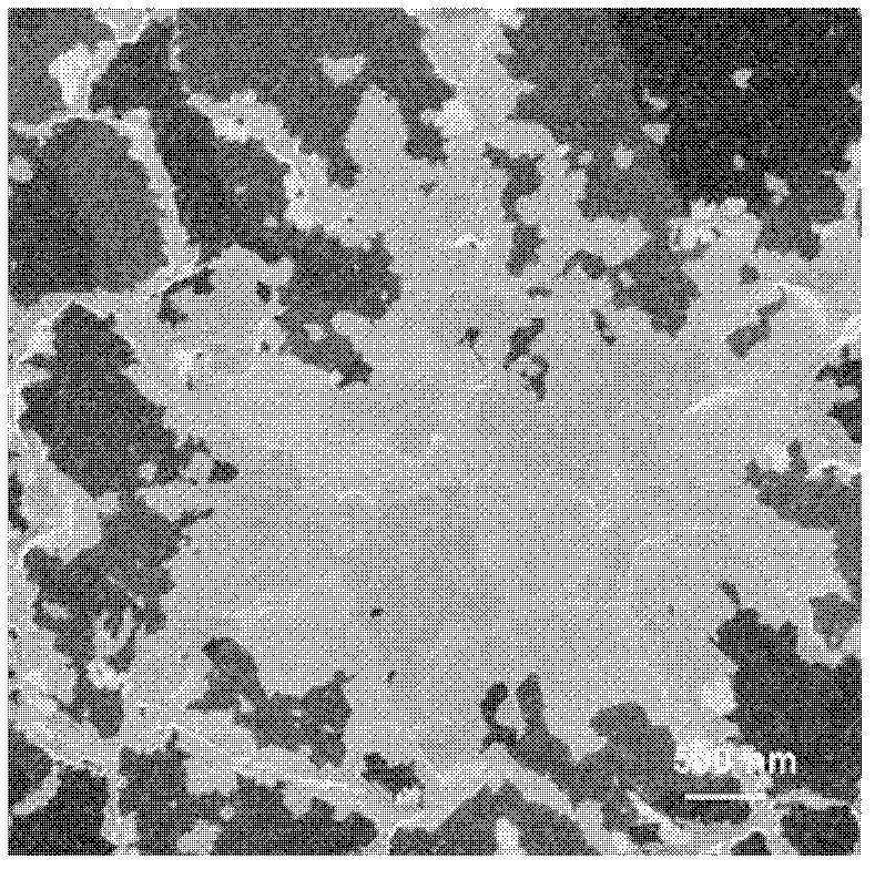
[0034] It includes the following steps: transfer n-type Si(100) to an ultra-high vacuum chamber, heat treat at 600°C for 300min, and then raise the temperature to 1000°C for 3 times, each time for 0.5min, so as to obtain a clean Si(100) surface; keep the substrate The temperature of the bottom Si(100) is 800°C, and H is passed into the ultra-high vacuum chamber 2 with C 2 h 4 mixed gas, and use the electron beam from the electron gun to C 2 h 4 Ionize into active carbon atom groups, and grow graphene film on Si(100) substrate for 5 minutes; finally, the substrate temperature has been lowered at a rate of 20°C / min to 25°C, thereby growing a large-area layer on the Si substrate The number is inconsistent (ranging from 1-3 layers) graphene film. image 3 A scanning electron microscope image of a graphene film grown on a single crystal Si substrate.

[0035] Effect: Si is the core material of contemporary silico...

Embodiment 2

[0038] Embodiment 2: prepare graphene film on polymer polyethylene terephthalate (PET) substrate

[0039] It includes the following steps: the PET substrate is introduced into the ultra-high vacuum chamber, the temperature of the PET substrate is 150°C, methane is passed into the ultra-high vacuum chamber, and the air pressure is kept at 8×10 -4 Torr, using an ion gun to ionize methane with an accelerating voltage of 1keV, so that the ionized methane is deposited on the PET substrate, the deposition time is 5min, and then the sample is annealed for 60min at a temperature of 100°C and synthesized on PET. A graphene film with a thickness of about 33.5nm (100 layers).

[0040]Effect: All kinds of flat panel displays, touch screens and solar cells need transparent electrode films. Flexible devices are attracting more and more attention. PET is a transparent flexible material, and transparent conductive graphene can be directly grown on PET at a relatively low temperature. It laid...

Embodiment 3

[0043] Embodiment 3: grow graphene film on polycrystalline copper substrate

[0044] It includes the following steps: mechanically polish a polycrystalline copper sheet with a thickness of 25 μm, spin-coat polymethyl methacrylate (PMMA) with a thickness of 100 nm on the polished Cu sheet, and transfer it to a high vacuum chamber (2×10 -5 torr), using RF beams to ionize PMMA, while raising the substrate temperature to 1050°C for 10 minutes, and finally lowering the substrate temperature to 25°C to synthesize single-layer graphene on the entire polycrystalline copper substrate. Figure 4 is the synthesized monolayer graphene transferred to SiO 2 Auger electron map on a substrate.

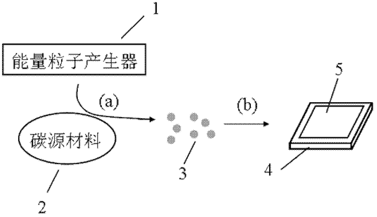
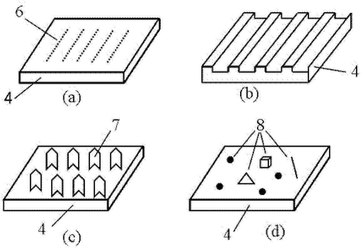
[0045] Effect: The technical method for generating active carbon atoms or carbon-containing active groups is energy particle technology, including but not limited to radio frequency treatment, laser treatment, electron beam treatment, neutron beam treatment, ion beam treatment, plasma treatment, micr...


PUM

PropertyMeasurementUnit
Thicknessaaaaaaaaaa
Widthaaaaaaaaaa
Thicknessaaaaaaaaaa

Abstract

The invention discloses a method for preparing a graphene film, comprising the steps of activating carbon atoms in carbon-containing gaseous carbon source, solid carbon source and liquid carbon source or a mixed carbon source material of any two or more than two of the carbon sources by adopting the technical methods of energy particles such as laser beam, electron beam, radio frequency beam, radial, photon, neutron beam, ion beam, plasma and the like; and forming the graphene film on a substrate. The method for producing the carbon atoms needed in the graphene film synthetizing is different from a conventional method and has the advantages that the method has great selectivity, and has no special requirement on the carbon source material and no special requirement on the substrate; the graphene film can be synthetized on the substrate which has the catalytic function and can be directly synthetized on the semiconductor or insulator substrate which does not have the catalytic function; and the formed graphene film is easily controlled in the aspects of the number of layers, structure and size and suitable for manufacturing high-performance photoelectronic devices on a large scale.

Description

technical field [0001] The invention relates to a graphene film, in particular to a method for synthesizing a graphene film. Background technique [0002] Graphene is a two-dimensional structure material composed of honeycomb single-layer carbon atoms, also known as single-layer graphite; in terms of physical properties, it is generally believed that the material with more than ten layers of graphene stacked is a three-dimensional structure of graphite, carbon nanotubes It is a one-dimensional nanomaterial made of graphene rolled into a barrel. Graphene has excellent two-dimensional electrical, optical, thermal, mechanical properties and chemical stability. Its unique two-dimensional structure and excellent crystallographic quality make it suitable for ultra-fast micro-nano optoelectronic devices, radio frequency devices, clean energy and various Sensors and other fields have important practical value. For example, electrons in graphene follow relativistic quantum mechanic...

Claims


Application Information

Patent Timeline
IPC IPC(8): C01B31/04B82Y40/00C01B32/184C01B32/186
Inventor 徐明生陈红征施敏敏吴刚汪茫
Owner ZHEJIANG UNIV
Why Eureka
Try Eureka