Method of preparing GaN monocrystal substrate in mechanical removal way

A gallium nitride single crystal and substrate technology, applied in chemical instruments and methods, single crystal growth, single crystal growth, etc., can solve problems such as complex equipment, affecting crystal quality, and separation difficulties, and achieve smooth surface without cracks, The effect of high crystal quality and simple equipment

Inactive Publication Date: 2013-04-03
PEKING UNIV
View PDF10 Cites 29 Cited by
  • Summary
  • Abstract
  • Description
  • Claims
  • Application Information

AI Technical Summary

Problems solved by technology

[0003] Due to the extremely high melting temperature and high nitrogen saturation vapor pressure, it is very difficult to prepare large-area GaN single crystals, and GaN-based devices have to be grown heterogeneously on substrates such as sapphire or silicon carbide with large mismatches.
Although this heteroepitaxy technology based on buffer layer technology has achieved great success, this method cannot give full play to the superior performance of GaN-based semiconductor materials. The main problems are: 1. Due to the large gap between GaN and sapphire The lattice mismatch and thermal stress mismatch, resulting in 10 9 cm -2 The misfit dislocations seriously affect the crystal quality and reduce the luminous efficiency of LED; 2. Sapphire is an insulator, and its resistivity is greater than 10 at room temperature. 11 Ωcm, so that it is impossible to make a device with a vertical structure, usually only N-type and P-type electrodes can be made on the upper surface o

Method used


Image

  • Method of preparing GaN monocrystal substrate in mechanical removal way
  • Method of preparing GaN monocrystal substrate in mechanical removal way
  • Method of preparing GaN monocrystal substrate in mechanical removal way

Examples


Embodiment 1

[0031] The preparation method of the gallium nitride single crystal substrate of this embodiment includes the following steps:

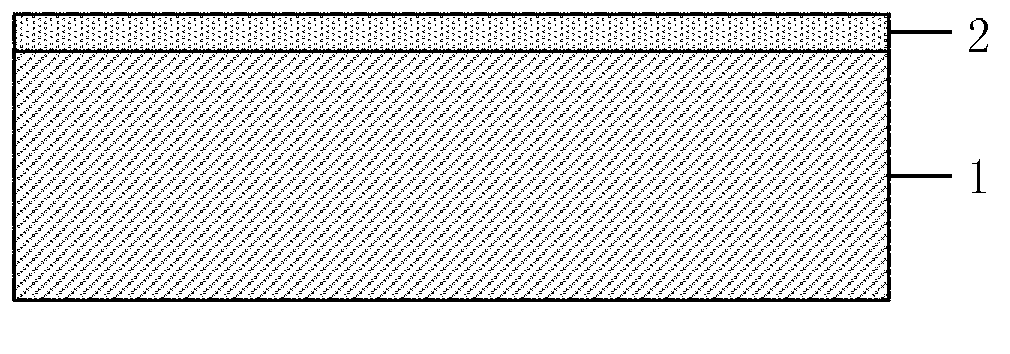
[0032]1) Using molecular beam epitaxy (MBE) to pre-deposit boron nitride h-BN film 2 on the surface of sapphire substrate 1: first, clean the surface of the commercial sapphire substrate with acetone, alcohol and deionized water, and wash the cleaned The sapphire substrate is placed in the MBE reaction chamber, and a hexagonal boron nitride film is deposited on the surface of the sapphire, with a thickness of 20nm, and the growth temperature is between 600~700°C, such as figure 1 shown;

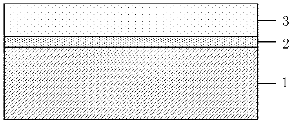
[0033] 2) Put it into the MOCVD reaction chamber for a growth to form a GaN single crystal film 3: first raise the temperature to a temperature lower than 600°C to grow a low-temperature buffer layer with a thickness of 30nm; then raise the temperature to 900~1100°C GaN is grown at high temperature to form a GaN single crystal film with a thickness of 4 μm, such as...

Embodiment 2

[0038] 1) Pre-deposit hexagonal boron nitride film h-BN on the surface of the sapphire substrate by magnetron sputtering: first, clean the surface of the commercial sapphire substrate with acetone, alcohol and deionized water; The sapphire substrate is placed in the reaction chamber of the magnetron sputtering apparatus, and a hexagonal boron nitride film is deposited on the surface of the sapphire, with a thickness of 20nm and a growth temperature of 600~700°C;

[0039] 2) Put it into the MOCVD reaction chamber for one growth to form a GaN single crystal film: first raise the temperature to a temperature lower than 600°C to grow a low-temperature buffer layer with a buffer layer thickness of 30nm; then raise the temperature to 900~1100°C to grow GaN at a high temperature , forming a GaN single crystal film with a thickness of 4 μm;

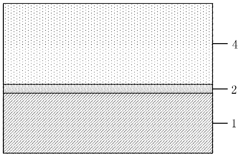
[0040] 3) Surface treatment before the secondary growth of HVPE, including organic cleaning and removal of the oxide layer; secondary growth of ...

Embodiment 3

[0043] 1) Using solid source molecular beam epitaxy (SSMBE) to pre-deposit graphene film on the surface of sapphire substrate: first, the surface of commercial sapphire substrate is cleaned with acetone, alcohol and deionized water, and the cleaned sapphire substrate is Put it into the SSMBE reaction chamber, deposit graphene film on the surface of sapphire, the thickness is 20nm, and the growth temperature is 600~700°C;

[0044] 2) Put it into the MOCVD reaction chamber for one growth to form a GaN single crystal film: first raise the temperature to a temperature lower than 600°C to grow a low-temperature buffer layer with a buffer layer thickness of 30nm; then raise the temperature to 900~1100°C to grow GaN at a high temperature , forming a GaN single crystal thick film with a thickness of 4 μm;

[0045] 3) Surface treatment before secondary growth of HVPE, including organic cleaning and removal of oxide layer; secondary growth of HVPE in HVPE reaction chamber to form GaN si...


PUM

PropertyMeasurementUnit
Thicknessaaaaaaaaaa
Growth temperatureaaaaaaaaaa

Abstract

The invention discloses a method of preparing a GaN monocrystal substrate in a mechanical removal way. A thin film of layered structure is pre-deposited between a GaN monocrystal thick film and a substrate and the GaN monocrystal thick film and the substrate are separated in a horizontal sliding mode to obtain a complete large size self-supporting GaN monocrystal substrate by utilizing the fact that the van der Waals force of the film of layered structure between the substrate and the GaN monocrystal thick film is weak and easy to slip. According to the method of preparation GaN monocrystal substrate in a mechanical removal way, a low-cost preparation method is utilized to obtain the self-supporting GaN monocrystal substrate which is smooth in surface without cracks and high-quality in crystal, the controllable separation of the GaN monocrystal thick film and the heterogeneous substrate is achieved with simple device with no need of other complex technology devices like the laser lift-off and the lithography etching nanometer graphics and no need of in situ etching or laser lift-off components in the reaction chamber, and the process stability, easy control and application to industrial production can be obtained.

Description

technical field [0001] The invention relates to the field of optoelectronic materials and devices, in particular to a method for preparing a gallium nitride single crystal substrate through a mechanical removal method. Background technique [0002] Gallium nitride GaN-based III~V nitrides are important wide-bandgap semiconductor materials with direct bandgap. It has broad application prospects in fields such as power electronic devices and other optoelectronic devices and electronic devices, as well as semiconductor devices under special conditions. [0003] Due to the extremely high melting temperature and high nitrogen saturation vapor pressure, it is very difficult to prepare large-area GaN single crystals, and GaN-based devices have to be grown heterogeneously on sapphire or silicon carbide substrates with large mismatches. Although this heteroepitaxy technology based on buffer layer technology has achieved great success, this method cannot give full play to the superio...

Claims


Application Information

Patent Timeline
IPC IPC(8): H01L21/78C30B33/00C30B25/18C30B23/02C30B29/40
Inventor 吴洁君王新强张国义于彤军康香宁
Owner PEKING UNIV
Why Eureka
Try Eureka