Organic light-emitting diode (OLED) device

A device and anti-reflection layer technology, applied in the field of OLED devices, can solve the problems of poor light transmittance, low work function light transmittance, and high work function of the transparent cathode structure, so as to improve stability, improve quantum efficiency, and improve luminous efficiency. Effect

Active Publication Date: 2013-04-03
KUNSHAN VISIONOX DISPLAY TECH +2
View PDF11 Cites 15 Cited by
  • Summary
  • Abstract
  • Description
  • Claims
  • Application Information

AI Technical Summary

Problems solved by technology

[0004] For this reason, what the present invention is to solve is the technical problem of high work function and poor light transmittance of the transparent cat

Method used


Image

  • Organic light-emitting diode (OLED) device
  • Organic light-emitting diode (OLED) device
  • Organic light-emitting diode (OLED) device

Examples


Embodiment 1

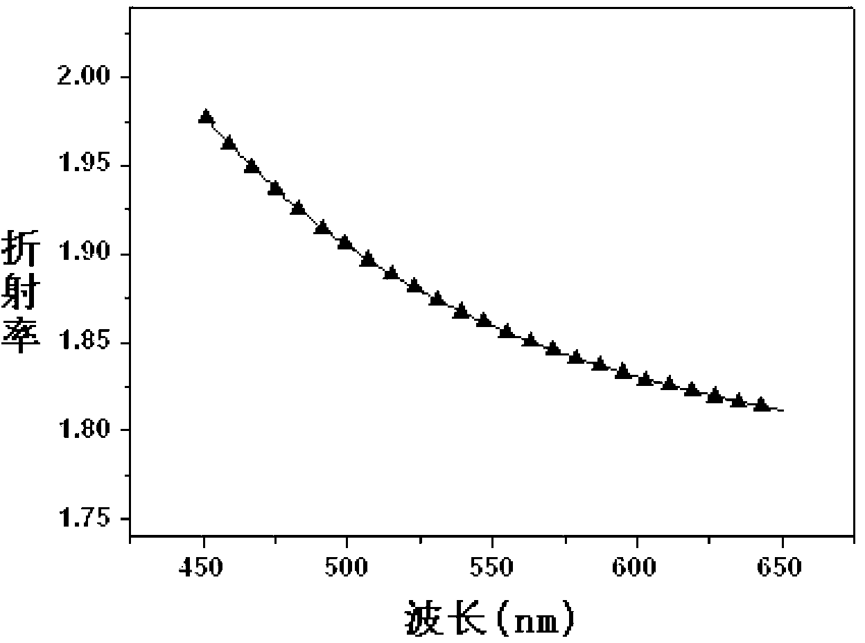
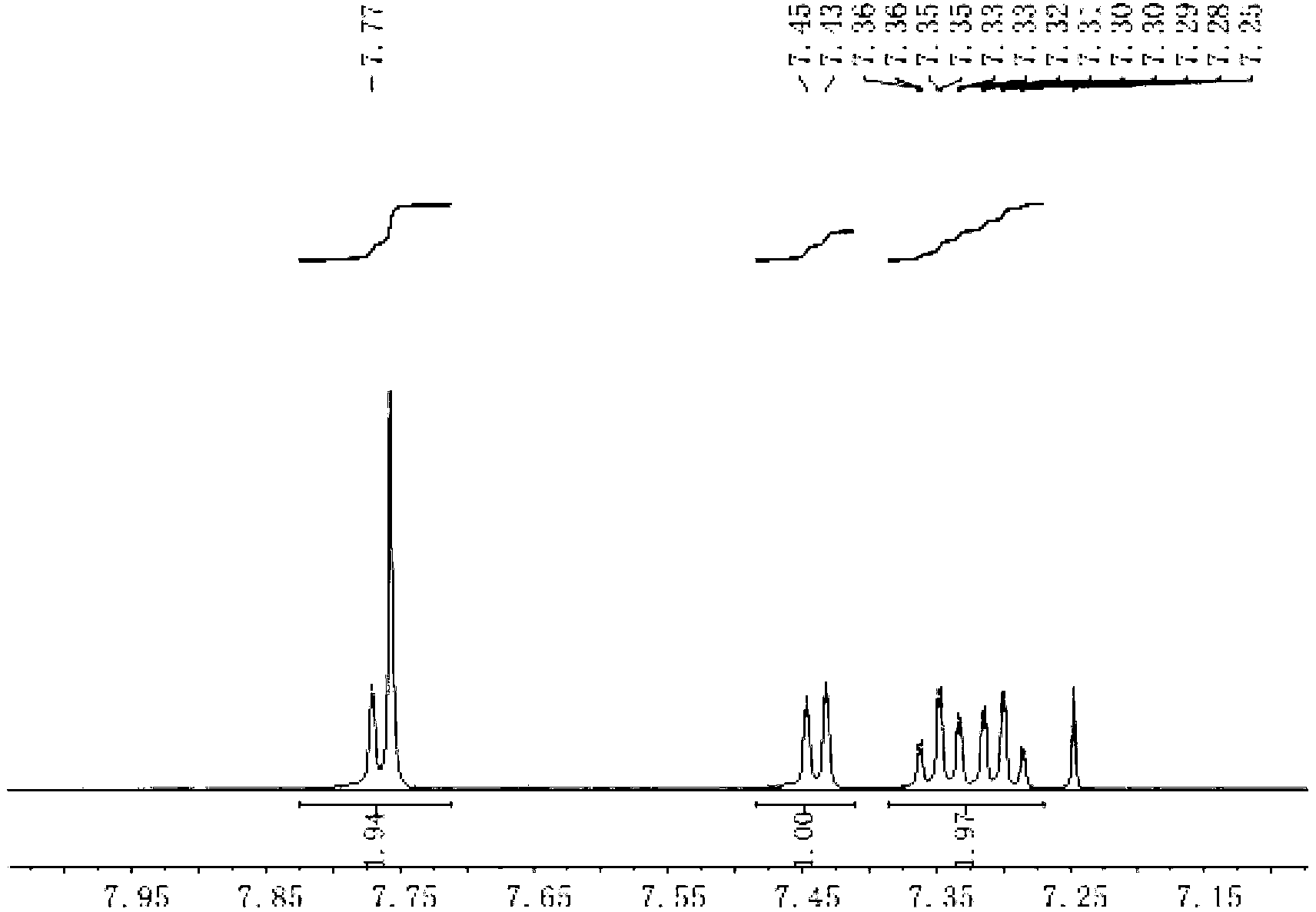
[0042] This embodiment is an embodiment of the preparation of the anti-reflection layer material F1.

[0043] The reaction route is divided into two steps. The first step is the preparation of the intermediate dibromoindenofluorene. The synthetic route is shown in the following formula:

[0044]

[0045] The specific method is:

[0046]Dissolve 26.4g 1,4-dibromo-2,5-dimethylbenzene and 24.4g phenylboronic acid in 300.0mL toluene and 100.0mL ethanol, add 27.6g K 2 CO 3 and 0.65g of tetrabutylammonium bromide, 1.5g of tetrakis(3-phenylphosphine)palladium, and reflux for 2h to finally obtain 22.5g of 2,5-dimethyl-4-phenylbiphenyl with a yield of 87.2%. Continue the reaction of the obtained product in the next step, dissolve it in 200.0 mL of pyridine, add 41.2 g of potassium permanganate and 50.0 mL of water, reflux for 2 h, and the reaction is complete. After filtering, the pyridine layer was made acidic with hydrochloric acid, and a large amount of white solid was found t...

Embodiment 2

[0057] This example is a preparation example of compound F2. The preparation of F2 includes two steps. The first step is the preparation of the intermediate dibromoindenofluorene, which is the same as in Example 1. The second step is the preparation of compound F2. Synthetic route As shown in the following formula:

[0058]

[0059] The specific method is:

[0060] A.25.2g (75mmol) N-p-tolyl-3-bromocarbazole was dissolved in 300ml redistilled THF, cooled the reaction system to -78°C with a cold bath, and slowly added 37.5ml of 2.4 M n-BuLi solution, after the dropwise addition is complete, keep this temperature for about 1 hour. Then 28ml of triisopropyl borate was added dropwise. After the drop, the reaction was stirred for 30 minutes, the cold bath was removed, the reaction system was slowly raised to room temperature and continued to stir at room temperature for 1.5 hours. Add 20ml of 1:1 hydrochloric acid solution dropwise to neutralize the reaction system, continue s...

Embodiment 3

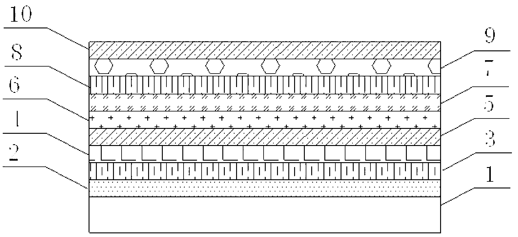
[0064] This embodiment is an example of OLED device preparation. The device in this embodiment is a top-emitting organic electroluminescent device. The structure includes: a substrate 1, and a reflective layer 2, an anode 3, and a hole injection layer formed by plating on the substrate 1 in sequence. layer (HIL) 4 , hole transport layer (HTL) 5 , light emitting layer (EML) 6 , electron transport layer (ETL) 7 , electron injection layer (EIL) 8 , cathode 9 and cover layer 10 .

[0065] Among them, the substrate 1 is a glass substrate, a quartz substrate or a flexible polymer substrate (plastic or polyimide, etc.); the reflective layer 2 can be metal silver or silver alloy, metal aluminum or aluminum alloy layer, used to reflect the direction of the incident substrate light; the anode layer 3 can be organic semiconductor materials such as ITO (indium tin oxide), IZO (indium zinc oxide), high work function metals or alloys, and C60; all of which can achieve the purpose of the pres...


PUM

PropertyMeasurementUnit
Thicknessaaaaaaaaaa
Thicknessaaaaaaaaaa
Thicknessaaaaaaaaaa

Abstract

The invention relates to an organic light-emitting diode (OLED) device which comprises a substrate and an anode, an organic layer and a cathode which are sequentially arranged on the substrate. The cathode is a transparent composite cathode and comprises an alloy layer of low work function metal and silver, a silver layer and an anti-reflection layer arranged on the silver layer. The work function of the low work function metal is smaller than 3.7eV, the molar ratio of the low work function metal and the silver in the alloy layer is 2:1-8:1, the thickness of the alloy layer is 3-11nm, the thickness of the silver layer is 15-30nm, and the thickness of the anti-reflection layer is 30-100nm. Magnesium, lithium, potassium and the like can be wrapped on the periphery of silver atoms when being evaporated with the silver together, the work function of the cathode can be effectively reduced by evaporation in proper proportion, and the cathode cannot absorb a large amount of visible light. The anti-reflection layer increases intensity of transparent light, is large in energy gap and does not affect color purity of the device. The thickness of the alloy layer and the silver layer is low, so that the alloy layer and the silver layer have high light transmittance.

Description

technical field [0001] The invention relates to the field of organic electroluminescent devices, in particular to an OLED device with a transparent composite cathode. Background technique [0002] Organic electroluminescent devices (English full name Organic Light-Emitting Diode, referred to as OLED) are divided into bottom-emitting devices (English full name is Bottom Organic Light-emitting Device, referred to as BEOLED) and top-emitting devices (English full name is TOPOrganic) according to the light emitting method. Light-emitting Device, referred to as TEOLED). The anode used in BEOLED is transparent. Generally, transparent indium tin oxide ITO (or indium zinc oxide IZO, etc.) is grown on a transparent substrate by sputtering as an anode. Transparent substrate injection. The display screen manufactured in this way has a relatively reduced area of ​​the display area and a lower aperture ratio of the display screen because the driving circuit and the display area are man...

Claims


Application Information

Patent Timeline
IPC IPC(8): H01L51/52H01L51/54
Inventor 邱勇刘嵩何麟
Owner KUNSHAN VISIONOX DISPLAY TECH
Why Eureka
Try Eureka