Organic-two-dimensional crystal-inorganic hybrid heterojunction solar cell device and preparation method thereof

A technology for solar cells and two-dimensional crystals, applied in the field of solar cells, can solve the problems of reducing the short-circuit current of solar cells, hindering charge transfer, reducing cell efficiency, etc., to enhance charge transfer capability, improve stability, and improve surface density of states defects. Effect

Active Publication Date: 2013-09-11
SUZHOU INAINK ELECTRONICS MATERIALS CO LTD
View PDF4 Cites 12 Cited by
  • Summary
  • Abstract
  • Description
  • Claims
  • Application Information

AI Technical Summary

Problems solved by technology

However, when naturally occurring SiO X When the thickness of the oxide layer is too thick, the oxide layer will form a charge barrier, which hinders the transmission of charges and simultaneously reduces the short-circuit current, open-circuit voltage and fill factor of the solar cell, thereby reducing the efficiency of the cell.
Therefore, the photoelectric conversion efficiency of this type of solar cell is not too high, and the highest efficiency is only about 10%.

Method used


Image

  • Organic-two-dimensional crystal-inorganic hybrid heterojunction solar cell device and preparation method thereof
  • Organic-two-dimensional crystal-inorganic hybrid heterojunction solar cell device and preparation method thereof
  • Organic-two-dimensional crystal-inorganic hybrid heterojunction solar cell device and preparation method thereof

Examples


preparation example Construction

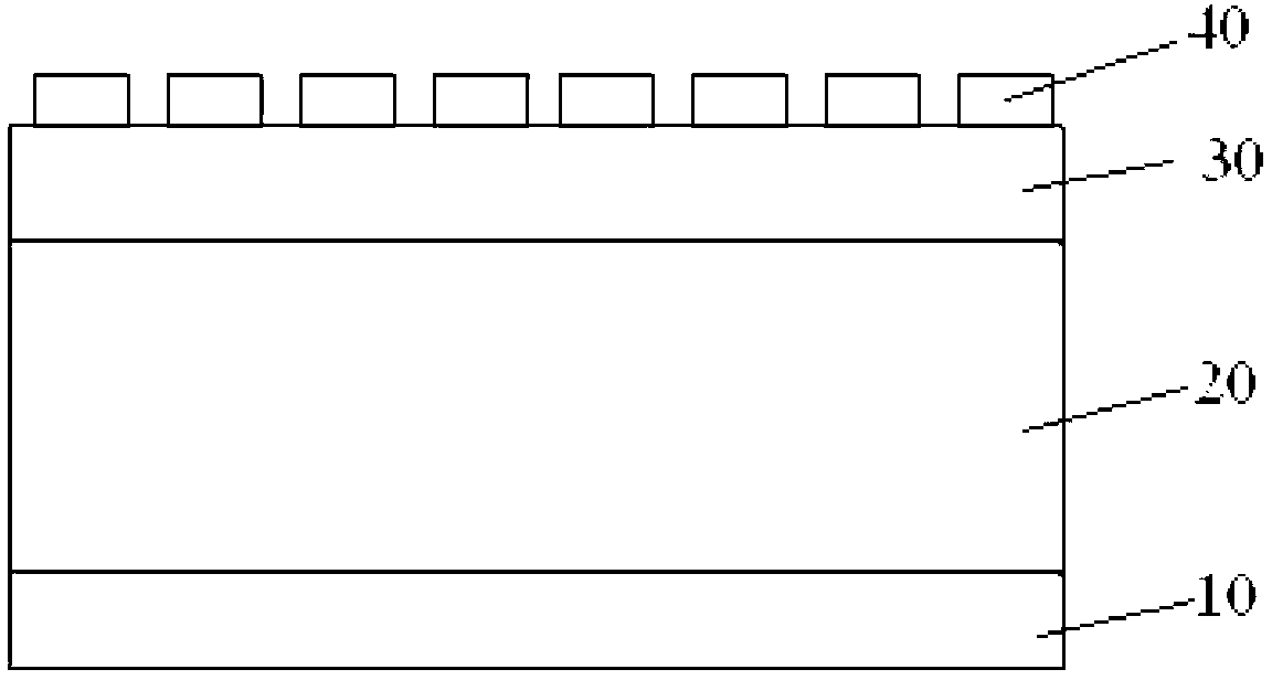
[0046] Correspondingly, the method for preparing an organic-two-dimensional crystal-inorganic hybrid heterojunction solar cell device in an embodiment of the present invention includes the following steps:

[0047] S1. Clean the silicon wafer and do an alkyl passivation treatment to obtain a silicon-based substrate;

[0048] S2. The two-dimensional layered nanocrystalline material and the conjugated organic substance in different proportions are fully stirred in a solvent to obtain a mixed solution. The solvent can be an alkyl alcohol solvent such as isopropanol, ethanol, or deionized water; the concentration of the mixed solution is 1 mg / mL;

[0049] S3. Spin-coating a mixed solution of two-dimensional layered nanocrystalline materials and conjugated organics in different proportions onto the surface of the silicon-based substrate by a homogenizing spin coating method. In the homogenizing spin coating method, the spin coating speed is 1800~2000 rpm, and the spin coating time is 1 m...

Embodiment 1

[0061] (1) Take a certain amount of Bi 2 Te 3 Dry and weigh for later use. The optical image in bright field and dark field is like Figure 4a , Figure 4b , Scanning electron micrograph and Raman spectroscopy such as Figure 5a , Figure 5b Shown

[0062] (2) Soak the n-type silicon wafer in the diluted HF solution for at least 15 minutes, rinse with deionized water and blow dry with nitrogen, and put it in the glove box for later use;

[0063] (3) Combine PEDOT:PSS solution with Bi 2 Te 3 Mix well and stir, and then spin coat a layer of PEDOT:PSS-Bi on the silicon wafer at a speed of 2000 rpm 2 Te 3 The film is then annealed at 125℃;

[0064] (4) In PEDOT:PSS-Bi under high vacuum 2 Te 3 An Ag electrode with a thickness of 200nm is thermally vaporized on the thin film, and an Al electrode is thermally vaporized on the back of the silicon wafer;

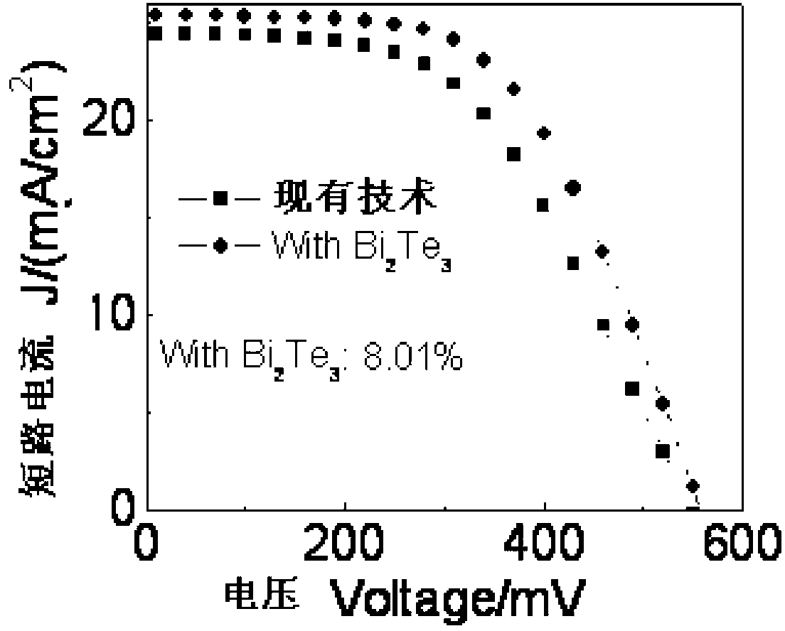
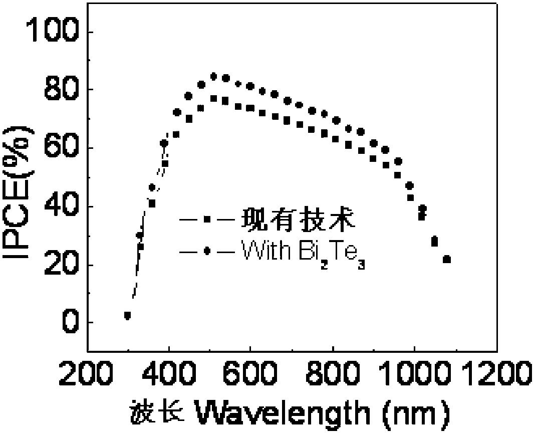
[0065] At room temperature, use xenon lamp to simulate sunlight AM1.5, light intensity 100mWcm -2 Under the conditions, the short-circuit cu...

Embodiment 2

[0067] (1) Take a certain amount of Bi 2 Te 3 Dry and weigh for later use. The optical image in bright field and dark field is like Figure 4a , Figure 4b , Scanning electron micrograph and Raman spectroscopy such as Figure 5a , Figure 5b Shown

[0068] (2) Soak the n-type silicon wafer in the diluted HF solution for at least 15 minutes, then rinse with deionized water and blow dry with nitrogen, put it in the glove box, and use the two-step chlorination / alkylation method to treat the silicon The chip is methylated, that is, the silicon chip is first put into a saturated phosphorus pentachloride chlorobenzene solution at 110 ± 10 ℃ for 1 hour, and then passed through the chlorobenzene washing solution (2 times) and tetrahydrofuran washing solution (2 times) After cleaning, transfer to methyl magnesium chloride (CH 3 MgCl) in tetrahydrofuran solution (1M), let stand at 70±10℃ for 12h;

[0069] (3) Combine PEDOT:PSS solution with Bi 2 Te 3 Mix well and stir, and then spin coat a l...


PUM


Abstract

The invention discloses an organic-two-dimensional crystal-inorganic hybrid heterojunction solar cell device and a preparation method thereof. The solar cell device comprises a metal back electrode, an n-type silicon-based substrate, an organic conjugated film uniformly mixed by conjugated organic matters and two-dimensional laminar nanocrystalline materials and metal gate electrodes sequentially from bottom to top. The surface of the silicon-based substrate is coated with mixed solution of the two-dimensional laminar nanocrystalline materials and the conjugated organic matters in a spin manner, or the two-dimensional laminar nanocrystalline materials and the conjugated organic matters of different concentrations are coated on the surface of the silicon-based substrate directly and sequentially in a spin manner to serve as a hole transport layer; stability of cells are improved by modification of an organic-inorganic matter hybrid heterojunction, charge transport capability of the solar cells is enhanced, surface state density defects are overcome effectively, and the solar cell device is simple to operate and easy for industrial production.

Description

Technical field [0001] The invention relates to the technical field of solar cells, in particular to an organic-two-dimensional crystal-inorganic hybrid heterojunction solar cell device and a preparation method thereof. Background technique [0002] With the rapid economic development, oil, coal, natural gas and other non-renewable resources have been declining. Research and use of renewable resources are becoming more and more important. There are many kinds of renewable resources, such as nuclear energy, solar energy, bioenergy, hydroelectric power, wind energy, geothermal energy and tidal energy. Among the many new energy sources, solar energy has become the focus of research and development and utilization of new energy with its unique advantages such as abundant reserves, no geographical restrictions, clean and pollution-free, fastest growth, most environmentally friendly, and inexhaustible. With the development of science and technology, a series of solar energy equipment...

Claims


Application Information

Patent Timeline
Patent Type & Authority Applications(China)
IPC IPC(8): H01L51/44H01L51/46H01L51/48
CPCY02E10/549Y02P70/50
Inventor 张杰孙宝全鲍桥梁
Owner SUZHOU INAINK ELECTRONICS MATERIALS CO LTD
Why Eureka
Try Eureka