A method for preparing a highly smooth and hard tin film with controllable wettability
A wettability and thin film technology, applied in the field of preparing high-smooth and high-hard TiN thin films with controllable wettability, can solve the problems of particle sputtering, affecting the decorative properties of thin films, weak atomic activity, etc. Good application prospect, simple and easy-to-implement effect
- Summary
- Abstract
- Description
- Claims
- Application Information
AI Technical Summary
Problems solved by technology
Method used
Image
Examples
Embodiment 1
[0033] In this embodiment, the HIPIMS technology is used to deposit a TiN thin film on the surface of the substrate. The deposition process is as follows: the substrate surface is first etched, then a Ti transition layer is deposited, and finally the TiN thin film is deposited, as follows.
[0034] Put the cleaned and dried substrate into the cavity and start vacuuming, when the vacuum degree reaches 4.0×10 -3 Pa, pass argon gas into the chamber to make the air pressure in the chamber 10.0mTorr, apply pulse negative bias voltage -400V to the substrate, and use glow discharge to etch the substrate for 30min; after the etching is completed, adjust the argon gas pressure to 2.0mTorr, turn on the high-power pulsed magnetron sputtering source to deposit Ti transition layer, the high-power pulsed magnetron sputtering source is powered by DC and pulse parallel connection, DC current 3A, pulse voltage 600V, pulse frequency 100Hz, pulse width 200μs , the substrate pulse negative bias v...
Embodiment 2
[0038] In this example, HIPIMS technology is used to deposit TiN film on the surface of the substrate. The deposition process and specific deposition conditions are basically the same as those in Example 1. The difference is that when depositing the TiN film on the surface of the substrate, the pulse negative bias of the substrate is adjusted to -350V , instead of -200V in Example 1.
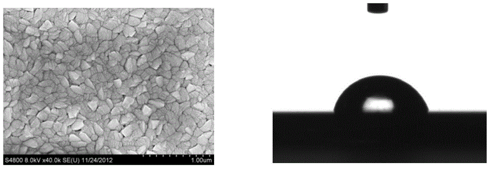
[0039] The surface topography and contact angle diagrams of the TiN film on the surface of the substrate prepared above are as follows: figure 2 shown. Compared figure 1 and figure 2Afterwards, it was found that when the TiN thin film was deposited, when the substrate pulse negative bias was adjusted, that is, when it was adjusted from -200V in Example 1 to -350V in Example 2, the surface topography of the TiN thin film changed, and its contact angle It also changed accordingly. Therefore, by adjusting the negative bias of the substrate pulse, the surface microstructure of the TiN film can...
Embodiment 3-6
[0042] In embodiment 3-6, adopt HIPIMS technology to deposit TiN thin film on substrate surface, its deposition process and concrete deposition condition are basically the same as embodiment 1, difference is: when substrate surface deposits TiN thin film, adjust substrate pulse negative bias to be -50V, -100, -300, -400 instead of -200V in Example 1.
[0043] similar figure 2 , the surface topography and contact angle diagrams of the TiN film on the surface of the substrate prepared above are compared with figure 1 After comparison, it is found that when the TiN film is deposited and the substrate pulse negative bias is adjusted, the surface topography of the TiN film changes, and its contact angle also changes accordingly. Therefore, by adjusting the negative bias of the substrate pulse, the surface microstructure of the TiN film can be changed, thereby preparing a TiN film with controllable wettability.
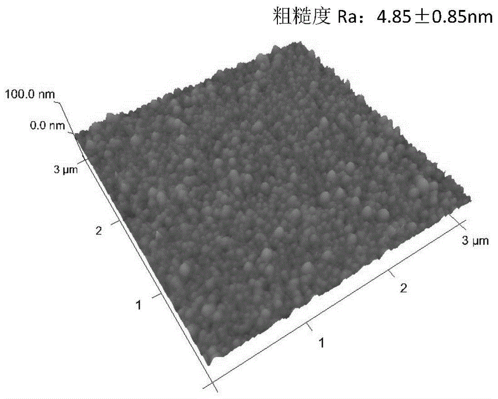
[0044] similar Figure 5 and 6 As shown, the AFM schematic diagra...
PUM
 Abstract
Description
Claims
Application Information


