High depth width ratio TSV through hole step-by-step etching and side wall modification method
A modification method and aspect ratio technology, applied in the field of microelectronics, can solve the problems of CMOS process line pollution, difficulty in removing the oxide layer, and breakage of the insulating layer seed layer, so as to reduce the difficulty of the process, solve the problem of large top leakage, increase reliability effect
- Summary
- Abstract
- Description
- Claims
- Application Information
AI Technical Summary
Problems solved by technology
Method used
Image

Examples
Embodiment 1
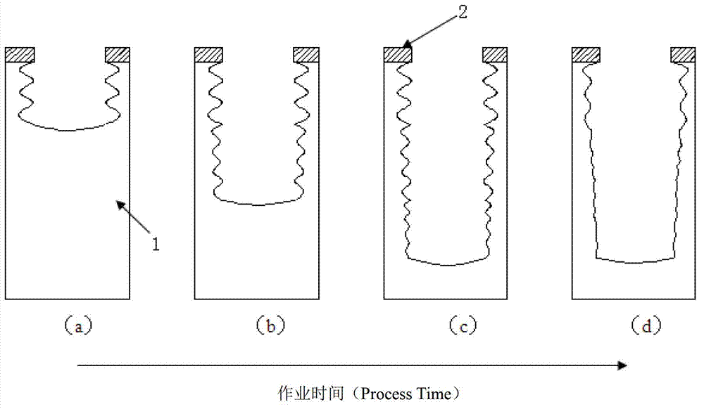
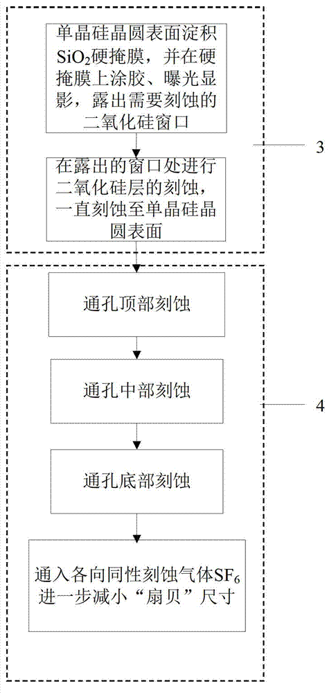
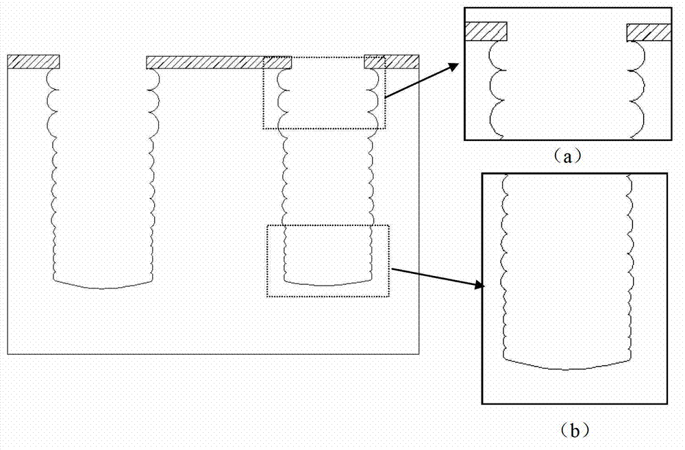
[0040] This embodiment is used for the fabrication of TSV via holes with a diameter of 10 μm and an aspect ratio of 10:1. The hole etching material is P type silicon, and the mask is 1μm thick SiO 2 . The ICP etching machine model is Alcatel AMS-100, and the specific steps according to the present invention are as follows (see image 3 ):
[0041] 1. First, deposit a layer of 1 μm SiO on the surface of the P type single crystal silicon wafer by PE CVD method 2 , and on SiO 2 The surface is coated with photoresist, exposed and developed to expose the silicon dioxide window to be etched (the window pattern is a circular hole with a diameter of 10 μm).
[0042] 2. Then use plasma dry etching to etch the silicon dioxide layer at the exposed window until it reaches the surface of the single crystal silicon wafer.
[0043] 3. Then carry out the optimized multi-step Bosch etching process proposed by the present invention, and the etching gas uses SF 6 , passivation gas using C ...
Embodiment 2
[0049] This embodiment is used for the fabrication of TSV via holes with a diameter of 5 μm and an aspect ratio of 10:1. The hole etching material is P type silicon, and the mask is 1.5μm thick SiO 2 . The ICP etching machine model is Alcatel AMS-100, and the specific steps according to the present invention are as follows (see image 3 ):
[0050] 1. First, deposit a layer of 1.5 μm SiO on the surface of the P type single crystal silicon wafer by PE CVD method 2 , and on SiO 2 The surface is coated with photoresist, exposed and developed to expose the silicon dioxide window to be etched (the window pattern is a circular hole with a diameter of 5 μm).
[0051] 2. Then use plasma dry etching to etch the silicon dioxide layer at the exposed window until it reaches the surface of the single crystal silicon wafer.
[0052] 3. Then carry out the optimized multi-step Bosch etching process proposed by the present invention, and the etching gas uses SF 6 , passivation gas using ...
Embodiment 3
[0058] This embodiment is used for the fabrication of TSV via holes with a diameter of 30 μm and an aspect ratio of 10:1. The hole etching material is P type silicon, and the mask is 1.5μm thick SiO 2 . The ICP etching machine model is Alcatel AMS-100, according to the concrete steps of the present invention, the steps are as follows:
[0059] 1. First, deposit a layer of 1.5 μm SiO on the surface of the P type single crystal silicon wafer by PE CVD method 2 , and on SiO 2The surface is coated with photoresist, exposed and developed, and the silicon dioxide window to be etched is exposed (the window pattern is a circular hole with a diameter of 30 μm).
[0060] 2. Then use plasma dry etching to etch the silicon dioxide layer at the exposed window until it reaches the surface of the single crystal silicon wafer.
[0061] 3. Then carry out the optimized multi-step Bosch etching process proposed by the present invention, and the etching gas uses SF 6 , passivation gas using ...
PUM
| Property | Measurement | Unit |
|---|---|---|
| Hole diameter | aaaaa | aaaaa |
Abstract
Description
Claims
Application Information
 - Generate Ideas
- Intellectual Property
- Life Sciences
- Materials
- Tech Scout
- Unparalleled Data Quality
- Higher Quality Content
- 60% Fewer Hallucinations
Browse by: Latest US Patents, China's latest patents, Technical Efficacy Thesaurus, Application Domain, Technology Topic, Popular Technical Reports.
© 2025 PatSnap. All rights reserved.Legal|Privacy policy|Modern Slavery Act Transparency Statement|Sitemap|About US| Contact US: help@patsnap.com