Method for preparing hexagonal boron nitride film

A hexagonal boron nitride, thin film technology, applied in gaseous chemical plating, metal material coating process, coating and other directions, can solve the uneven thickness of hexagonal boron nitride continuous film, between tens of nanometers to ten microns , it is difficult to meet the needs of the application and other problems, to achieve the effect of low cost, wide window and good crystallinity

Active Publication Date: 2014-05-07
SHANGHAI INST OF MICROSYSTEM & INFORMATION TECH CHINESE ACAD OF SCI
View PDF3 Cites 26 Cited by
  • Summary
  • Abstract
  • Description
  • Claims
  • Application Information

AI Technical Summary

Problems solved by technology

However, the thickness of the hexagonal boron nitride continuous film prepared is generally very uneven, and the number of atomic layers generally ranges from 2 to 10; the isolated hexagonal boron nitride crystal domains prepared by low-pressure growth on substrates such as Cu and Ni, although It has a high monolayer coverage, but the crystal domain size is generally small, generally between tens of nanometers and ten microns, which is difficult to meet the needs of its application in the field of devices

Method used


Image

  • Method for preparing hexagonal boron nitride film
  • Method for preparing hexagonal boron nitride film
  • Method for preparing hexagonal boron nitride film

Examples


Embodiment 1

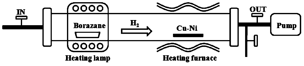
[0042] A copper-nickel alloy foil substrate is prepared first. In this embodiment, a copper foil with a thickness of 25 μm is selected. Preferably, the surface of the copper foil is polished using a classic electrochemical polishing process. Among them, the electrochemical polishing solution is a phosphoric acid solution with a volume ratio of 85%, and the current density is 0.2A / cm 2 , the polishing time is 1-2min. After polishing, use acetone and isopropanol to ultrasonically clean for 10min respectively, and then use a nitrogen gun to dry the polished copper foil to obtain a clean surface with a surface roughness below 50nm and a thickness of about 20μm. copper foil.

[0043] Then put the polished and cleaned copper foil on the figure 1 Annealed at 1050°C for 2h in the tube furnace shown. The annealing process is carried out under normal pressure, the selected atmosphere is hydrogen and argon, and the flow rate ratio Ar:H 2 =5:1, the partial pressure ratio of argon and h...

Embodiment 2

[0051] The difference between this embodiment and the first embodiment is that the growth time of the hexagonal boron nitride film in the first embodiment, that is, the heating time of the solid source ammonia borane is extended to 40 minutes, and the rest of the process parameters are the same as the first embodiment.

[0052] The results of this embodiment: as Figure 4 Shown, compared with embodiment one, along with the increase of growth time, reaction proceeds further, from Figure 4 It can be seen that the hexagonal boron nitride crystal domains are further enlarged, and the maximum side length can reach 60 μm. After the growth was completed, the prepared films were transferred to SiO 2 / Si substrate, its XPS (X Photoelectron Spectroscopy) spectrum is as follows Figures 5a-5c As shown, the binding energies of N1s and B1s are 398.1eV and 190.5eV, respectively, and the atomic ratio B:N=1:1.01, which confirms the existence of only B-N bonds in the film, which is consiste...

Embodiment 3

[0054] The difference between this embodiment and the first embodiment is that the growth time of the hexagonal boron nitride thin film in the first embodiment is extended to 60 minutes, and the temperature of the substrate during growth is increased to 1085° C., and the rest of the process is the same as the first embodiment.

[0055] Results of this example: by increasing the temperature on the surface of the copper-nickel alloy foil substrate during growth, the nucleation density of the hexagonal boron nitride crystal domain is reduced, and the size of the prepared crystal domain is further increased with the further increase of the growth time. Big. Such as Figure 6 As shown, the hexagonal boron nitride crystal domain side length prepared under this growth condition can reach up to 100 μm, which is an order of magnitude higher than that reported in the existing literature. It should be noted that with the increase of the size, the boundary of the crystal domain begins to...


PUM

PropertyMeasurementUnit
thicknessaaaaaaaaaa
surface roughnessaaaaaaaaaa
thicknessaaaaaaaaaa

Abstract

The invention provides a method for preparing a hexagonal boron nitride film. The method comprises the following steps of firstly preparing a copper-nickel alloy foil as a substrate; placing the substrate into a chemical vapor deposition cavity with the pressure intensity of 20-5000 Pa to preserve the temperature of the substrate between 950 DEG C and 1090 DEG C; introducing a source substance with the temperature of 50-100 DEG C, and introducing a protective gas to grow for 10 minutes-3 hours so as to prepare the hexagonal boron nitride film on the surface of the copper-nickel alloy foil substrate. The method provided by the invention can be used for preparing hexagonal boron nitride crystal domains with different sizes and continuous films with different thicknesses on the copper-nickel alloy foil substrate by controlling growth parameters. The prepared hexagonal boron nitride crystal domains can achieve the maximal side length of hundreds of micrometers, have the advantages of good crystallinity, simple preparation condition, low cost, wide window of a condition parameter required by growth and good repeatability and lays the foundation for the wide application of the hexagonal boron nitride film in the fields of a graphene device and the like.

Description

technical field [0001] The invention relates to the technical field of two-dimensional material preparation, in particular to a method for preparing large-sized hexagonal boron nitride crystal domains and thin films by using a copper-nickel alloy substrate through a chemical vapor deposition method. Background technique [0002] Hexagonal boron nitride (h-BN) is a typical two-dimensional planar material with a hexagonal network structure similar to graphene, composed of sp 2 Hybridized B atoms and N atoms alternately occupy the vertices of the hexagonal grid. Hexagonal boron nitride has a high band gap (5.97eV), high in-plane mechanical strength and high thermal conductivity, and strong chemical stability, making it have a very wide application prospect in transparent insulating films and other fields. Especially as a substrate insulating layer for graphene devices, graphene on hexagonal boron nitride substrates has comparable mobility to suspended graphene due to its atomi...

Claims


Application Information

Patent Timeline
Patent Type & Authority Applications(China)
IPC IPC(8): C23C16/34
Inventor 卢光远吴天如宋阳曦王浩敏谢晓明江绵恒
Owner SHANGHAI INST OF MICROSYSTEM & INFORMATION TECH CHINESE ACAD OF SCI
Why Eureka
Try Eureka