Method for preparing plurality of layers of superfine silicon lines

An ultra-fine silicon and line technology, which is applied in semiconductor/solid-state device manufacturing, nanotechnology for information processing, semiconductor devices, etc., can solve the problems of complex process and long production cycle, and achieve a large process window and process cost. Small, uniform cross-sectional topography

Active Publication Date: 2014-05-28
PEKING UNIV
View PDF4 Cites 8 Cited by
  • Summary
  • Abstract
  • Description
  • Claims
  • Application Information

AI Technical Summary

Problems solved by technology

However, the film thickness of each layer in the superlattice structure is limited by factors such as lattice mismatch and stress release, and the process is relatively complicated and the production cycle is relatively long

Method used


Image

  • Method for preparing plurality of layers of superfine silicon lines
  • Method for preparing plurality of layers of superfine silicon lines
  • Method for preparing plurality of layers of superfine silicon lines

Examples


Embodiment 1

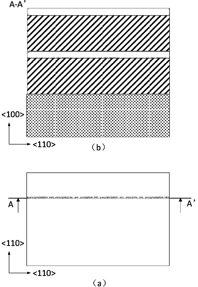
[0063] A two-layer nanowire structure with a diameter of about 5 nm can be achieved according to the following steps:

[0064] 1) ALD on (100) bulk silicon substrate SiO 2 as a sacrificial layer;

[0065] 2) ALD Si 3 N 4 as a corrosion mask;

[0066] 3) ALD SiO 2 as a sacrificial layer;

[0067] 4) ALD Si 3 N 4 As a corrosion mask, such as figure 1 shown;

[0068] 5) Electron beam lithography defines the epitaxial windows of Fin and the source and drain regions, in which the width of the Fin structure is 20nm, the length is 300nm, and the length direction and the sidewall crystal direction are both along ;

[0069] 6) Anisotropically etching the stacked structure of the sacrificial layer-masking layer, transferring the pattern defined by photolithography to the stacked structure, exposing the silicon substrate;

[0070] 7) Remove photoresist, such as figure 2 shown;

[0071] 8) Selective epitaxy silicon;

[0072] 9) Chemical mechanical polishing remove...

Embodiment 2

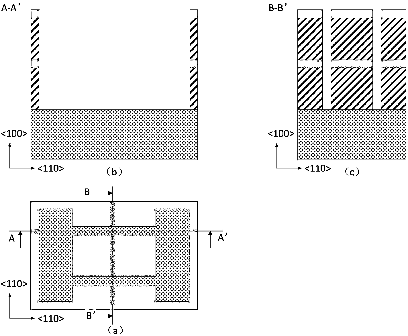
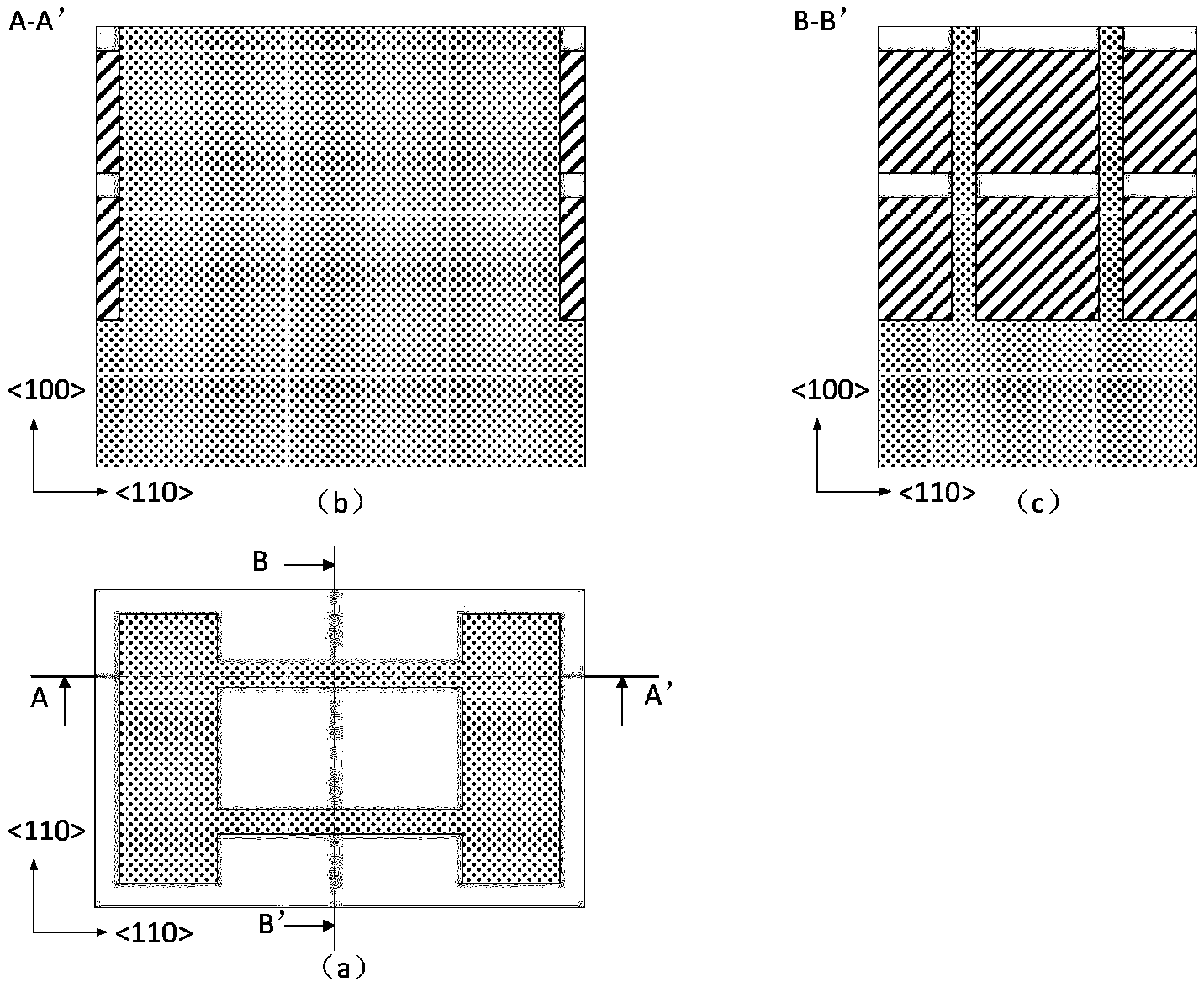
[0083] A three-layer nanowire structure with a diameter of about 10 nm was prepared.

[0084] With embodiment 1, difference is:

[0085] a) Select (110) SOI substrate;

[0086] b) Steps 1)-4), the sacrificial layer is made of ICPECVD Polycrystalline germanium, the mask layer is made of ICPECVD SiO 2 ;

[0087] c) After step 4), execute 4.1): ICPECVD Polycrystalline germanium as sacrificial layer; 4.2): ICPECVD deposition SiO 2 as a corrosion mask;

[0088] d) In step 5, 193nm immersion lithography is used to define the epitaxial windows of Fin and the source and drain regions, wherein the width of the Fin structure is 30 nanometers, the length is 300 nanometers, the length direction is along the crystal direction, and the sidewall is along the crystal orientation;

[0089] e) Step 8) Selective epitaxy silicon;

[0090] f) Step 10) using ICPECVD SiO 2 as the top masking layer;

[0091] g) Step 11) uses 193nm immersion lithography to define the etch window fo...


PUM

PropertyMeasurementUnit
diameteraaaaaaaaaa
lengthaaaaaaaaaa
diameteraaaaaaaaaa

Abstract

The invention relates to a method for preparing a plurality of layers of superfine silicon lines. The method comprises the following steps: preparing a silicon etching masking layer; extending to form Fin and source drain regions on two ends of the Fin; and forming the plurality of layers of superfine silicon lines. The method has the advantages that the positions of the superfine lines can be accurately defined through the deposition of an atomic layer, and the controllability is good; the anisotropy etching on silicon stops automatically, a process window is large, and the sections of nano lines obtained by etching are uniform and smooth in appearance; the process for forming a plurality of layers of side wall etching masks by a method of firstly preparing masks and then extending a channel is simple, and the plurality of layers of side wall masks can be obtained only by one etching of the extension window regardless of the number of masking layers; the lines with sizes of less than 10nm can be prepared by combining oxidization technology, thus meeting the requirement of the key process of small-sized devices; polycrystalline silicon can be subjected to wet etching with a TMAH solution, and the operation is simple, convenient and safe; metal ions are not introduced, and the method is applicable to the integrated circuit manufacturing technology; the method is entirely compatible with a bulk silicon planar transistor process, and the process cost is small.

Description

technical field [0001] The invention belongs to the technical field of ultra-large-scale integrated circuit manufacturing, and relates to a method for preparing ultra-fine silicon lines in integrated circuits, in particular to a method for preparing position and shape controllable by combining selective epitaxy of silicon and anisotropic etching of silicon method of multilayer ultrafine silicon lines. Background technique [0002] As Moore's Law advances to the 22nm process node, traditional planar devices have become increasingly prominent due to short-channel effects and reliability issues, resulting in serious degradation of device performance and failing to meet the requirements of Moore's Law. The three-dimensional multi-gate device (Multi-gate MOSFET, MuGFET) represented by the fin field effect transistor (FinFET), with its outstanding ability to suppress short-channel effects, high integration density, and compatibility with traditional CMOS processes, has been widely...

Claims


Application Information

Patent Timeline
Patent Type & Authority Applications(China)
IPC IPC(8): H01L21/02H01L21/336B82Y10/00
CPCH01L21/02603H01L29/0669
Inventor 黎明杨远程樊捷闻宣浩然张昊黄如
Owner PEKING UNIV
Why Eureka
Try Eureka