Double-face P-type crystalline silicon battery structure and manufacturing method thereof

A crystalline silicon cell, double-sided technology, applied in circuits, electrical components, photovoltaic power generation, etc., can solve problems such as unfavorable promotion and application of double-sided cells, lower production costs, unfavorable production efficiency, etc., to reduce production process costs and reduce density. , the effect of reducing the interface recombination rate

Active Publication Date: 2014-06-25
中国东方电气集团有限公司
View PDF5 Cites 20 Cited by
  • Summary
  • Abstract
  • Description
  • Claims
  • Application Information

AI Technical Summary

Problems solved by technology

In the above two reports, it is necessary to prepare a diffusion barrier layer first, remove the barrier layer after phosphorus diffusion, prepare a passivation layer on the boron diffusion surface, and then prepare a silicon nitr

Method used


Image

  • Double-face P-type crystalline silicon battery structure and manufacturing method thereof
  • Double-face P-type crystalline silicon battery structure and manufacturing method thereof

Examples


Embodiment 1

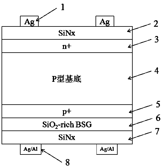
[0027] Adopt the method of the present invention to make a kind of double-sided P-type crystalline silicon battery structure, concrete steps are as follows:

[0028] (1) Czochralski monocrystalline P-type wafers are selected, with a resistivity of 1-5 ohm.cm. Both sides of the monocrystalline silicon wafers are cleaned and treated with positive pyramid texture to reduce the reflection of the final battery;

[0029] (2) Put the front surface of the above silicon wafer into a diffusion furnace for boron diffusion, using boron tribromide liquid source boron diffusion, the diffusion process is divided into deposition and advancement steps, the constant temperature zone is controlled at 900-960 during deposition and advancement The diffusion time is 30-60 minutes, and the placement method of the front surface veneer is to reduce the degree of boron diffusion on the front side of the silicon wafer as much as possible, and the boron diffusion resistance is controlled at 70-120 ohms / sq...

Embodiment 2

[0040] Adopt the method of the present invention to make a kind of double-sided P-type crystalline silicon battery structure, concrete steps are as follows:

[0041] (1) Czochralski monocrystalline P-type wafers are selected, with a resistivity of 1-3 ohm.cm. Both sides of the monocrystalline silicon wafers are cleaned and treated with positive pyramid texture to reduce the reflection of the final battery;

[0042] (2) Put the front surface of the above silicon wafer into a diffusion furnace for boron diffusion, using boron tribromide liquid source boron diffusion, the diffusion process is divided into deposition and advancement steps, the constant temperature zone is controlled at 900-960 during deposition and advancement The diffusion time is 30-60 minutes, and the placement method of the front surface veneer is to reduce the degree of boron diffusion on the front side of the silicon wafer as much as possible, and the boron diffusion resistance is controlled at 70-90 ohms / squ...


PUM

PropertyMeasurementUnit
Thicknessaaaaaaaaaa
Thicknessaaaaaaaaaa
Thicknessaaaaaaaaaa

Abstract

The invention discloses a double-face P-type crystalline silicon battery structure and a manufacturing method thereof. The double-face P-type crystalline silicon battery structure formed through the method comprises a back face passivation anti-reflecting composite film, the anti-reflecting composite film comprises a borosilicate glass layer containing SiO2 and a silicon nitride layer, the borosilicate glass layer is arranged on a double-face crystalline silicon battery boron diffusion layer, and the silicon nitride layer is deposited on the borosilicate glass layer; the battery structure can reduce the interface state density and the interface compounding rate and realize the passivation effect on the boron diffusion layer; a BSG/SiNx laminated structure formed by the borosilicate glass layer and the silicon nitride layer can realize the functions such as passivation, diffusion masking and reflection resisting, and can increase the open-circuit voltage of a battery, the short-circuit current of the battery and the photo-electric conversion efficiency of the battery; the BSG(SiO2-rich)/SiNx laminated structure is adopted in the back face to serve as the back face passivation layer, the diffusion masking layer and the back face anti-reflection layer of the battery, therefore, the technology is greatly simplified, the production efficiency is increased and the production technology cost is lowered.

Description

Technical field [0001] The invention involves the field of solar cell production technology, especially a double -sided P -shaped crystal silicon battery structure and its preparation methods. Background technique [0002] At present, crystal silicon batteries are the mainstream products of the solar cell market. Traditional crystalline silicon solar cells are based on P -type base batteries. They use P -shaped crystal silicon materials to form a PN knot in the front phosphorus of the substrate and sedify the reflex membrane.Aluminum paste is printed on the back to form a back field.In addition to the weight of solar battery surfaces directly from the solar radiation, it also includes a considerable indirect indirect radiation or scattering radiation component caused by air, dust, and sky suspension.The amount of 10-30 % of the amount is increased in the weather with insufficient sunlight.If the light can be transformed into electrical energy from the back of the battery into the...

Claims


Application Information

Patent Timeline
IPC IPC(8): H01L31/0216H01L31/18
CPCH01L31/02168H01L31/0684H01L31/1804H01L31/1868Y02E10/547Y02P70/50
Inventor 张中伟张小宾黄仑
Owner 中国东方电气集团有限公司
Why Eureka
Try Eureka