Atom gas cavity device based on MEMS technology and manufacturing method thereof

An atomic gas cavity and device technology, applied in chemical instruments and methods, instruments using atomic clocks, membrane technology, etc., can solve the problems of limited interaction optical path, low signal-to-noise ratio of CPT signals, difficulties, etc., to increase interaction The effect of space length, signal-to-noise ratio enhancement, and stability improvement

Inactive Publication Date: 2014-07-23
CHINA ELECTRONIC TECH GRP CORP NO 38 RES INST
View PDF8 Cites 16 Cited by
  • Summary
  • Abstract
  • Description
  • Claims
  • Application Information

AI Technical Summary

Problems solved by technology

The optical path length of the interaction between light and atoms in the alkali metal atom gas cavity structure of this structure is limited by the thickness of the silicon wafer and the silicon processing technology, usually 1 mm to 2 mm, and it is difficult and expensive to further increase the thickness, thus limiting the interaction between light and atoms. The action optical path, the signal-to-noise ratio of the CPT signal is low, which affects the frequency stability of the CPT atomic clock

Method used


Image

  • Atom gas cavity device based on MEMS technology and manufacturing method thereof
  • Atom gas cavity device based on MEMS technology and manufacturing method thereof
  • Atom gas cavity device based on MEMS technology and manufacturing method thereof

Examples


Embodiment 1

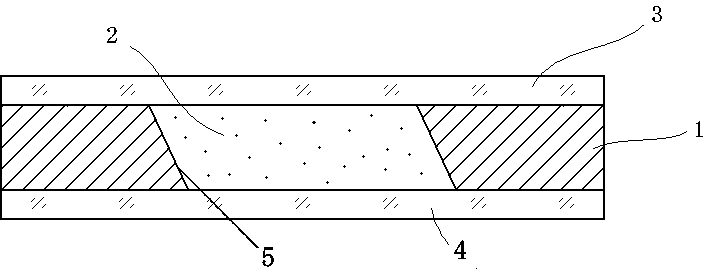
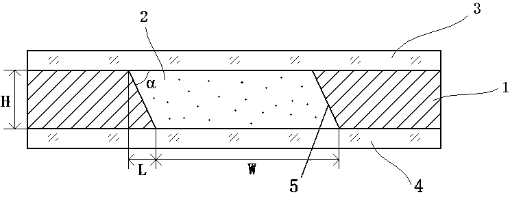
[0029] see figure 1 and figure 2 , the atomic gas cavity device based on MEMS technology has a typical sandwich structure, including a silicon wafer 1 with a through hole in the middle as the middle layer, and the cross section of the through hole is a parallelogram. One side of the silicon wafer 1 is provided with a top glass 3 , and the other side is provided with a bottom glass 4 . The two side walls of the parallelogram through hole are parallel slopes; the side walls of the slopes on both sides of the through hole are respectively provided with metal film reflectors 5 . The side walls of the slopes on both sides of the through hole are formed by anisotropic wet etching of silicon. The side walls of the through hole are {111} crystal planes of the silicon wafer 1, and the included angle with the top glass 3 or bottom glass 4 is 54.7 degrees. .

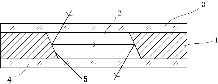
[0030] see image 3 , the optical path of the laser in the atomic gas cavity 2 device is mainly determined by the lateral w...

Embodiment 2

[0037] The structure of the atomic gas chamber device based on MEMS technology is the same as that in Embodiment 1.

[0038] Concrete preparation operation steps are as follows:

[0039] 1. Select a P(100) type silicon wafer 1 with a thickness of 1mm, use silicon nitride as a mask, and perform double-sided through-etching through the TMAH anisotropic wet etching process, and form a parallel cross section on the silicon wafer There are one hundred and fifty through holes in the quadrilateral, and the sidewalls on both sides of each through hole are {111} crystal planes, and the lateral width of the through holes is 5 mm. The temperature of TMAH corrosion is 80°C;

[0040] 2. Using a sputtering process and hard mask technology, metal film mirrors 5 are respectively fabricated on the side walls on both sides of each through hole;

[0041] 3. Carry out the first silicon-glass anode bonding to complete the bonding of the silicon wafer 1 and the bottom glass 4; at the same time, i...


PUM

PropertyMeasurementUnit
thicknessaaaaaaaaaa

Abstract

The invention relates to an atom gas cavity device based on an MEMS technology and a manufacturing method thereof. The atom gas cavity device has a typical sandwich structure and is of a cavity structure formed by defining a silicon wafer with through holes and two glass sheets in a bonding mode. The cross section of each through hole is a parallelogram and is formed by a monocrystalline silicon slice of an N(100) type through silicon anisotropism wet etching, and the side walls of each through hole are crystal faces{111} of the silicon wafer. The two glass sheets and the silicon wafer with the through holes form an atom gas cavity after silicon-glass anodic bonding. The atom gas cavity device can be used for systems of atomic clocks, magnetometers and the like, the distance between two reflectors in the cavity can be increased easily through changing of size design of the atom gas cavity, accordingly, the interaction space lengths between lasers and atom gas are increased, the signal to noise ratio of coherent layout imprisoned effect signals is enhanced, and improvement of stability of a system is facilitated.

Description

technical field [0001] The invention belongs to the technical field of micro-electro-mechanical system (MEMS) device manufacturing and packaging, and the technical field of atomic physics devices, and specifically relates to a micro-atomic cavity structure based on MEMS technology and a manufacturing method thereof. Background technique [0002] Atomic clocks can measure time with an accuracy of one billionth of a second or even higher. Atomic clocks are currently the most accurate artificial clocks, and their related research is of great significance. CPT (Coherent Population Trapping, coherent layout trapping effect) atomic clock is an atomic clock frequency source realized by using two-color coherent light to interact with atoms to prepare atoms into a coherent state, and using the CPT signal as a microwave frequency discrimination signal. Due to the characteristics of easy miniaturization, low power consumption and high frequency stability, the CPT atomic clock has been ...

Claims


Application Information

Patent Timeline
Patent Type & Authority Applications(China)
IPC IPC(8): G04F5/14B81B1/00B81C1/00B81C3/00
Inventor 许磊刘建勇王光池郑林华齐步坤王晓东
Owner CHINA ELECTRONIC TECH GRP CORP NO 38 RES INST
Why Eureka
Try Eureka