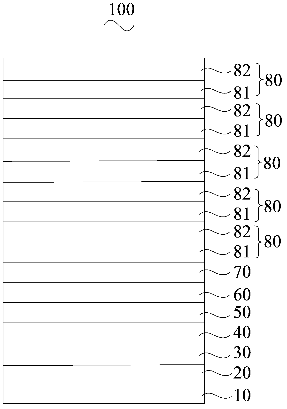
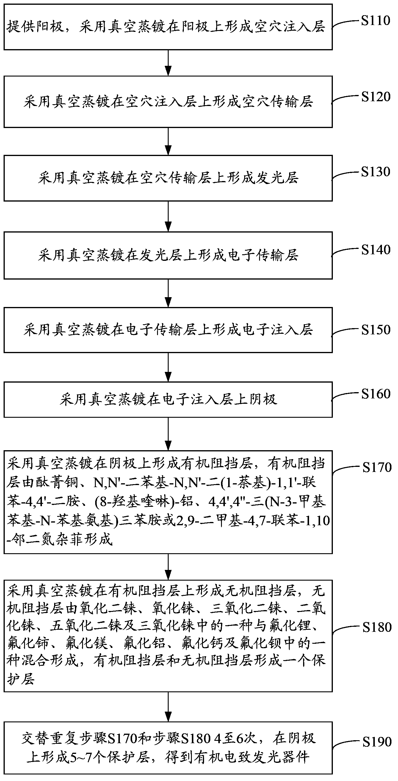
Organic electroluminescent device and packaging method thereof
A technology of electroluminescent devices and packaging methods, which is applied in the direction of organic semiconductor devices, organic semiconductor device materials, electric solid devices, etc., can solve the problems of short service life, poor stability, and easy to be corroded, and achieve high service life Effect
- Summary
- Abstract
- Description
- Claims
- Application Information
AI Technical Summary
Problems solved by technology
Method used
Image
Examples
Embodiment 1
[0094] The structure is ITO / MoO 3 :NPB / TCTA / Ir(ppy) 3 :TPBI / Bphen / CsN 3:Bphen / ZnS / Ag / ZnS / (CuPc / Re 2 O:NiS) 7 Encapsulation of organic electroluminescent devices
[0095] (1) Provide an anode, the anode is indium tin oxide glass, expressed as ITO. First, put the anode into acetone, ethanol, deionized water and ethanol for ultrasonic cleaning, each ultrasonic cleaning for 5 minutes, then blow dry with nitrogen, and then dry in an oven to obtain a clean and dry anode. Further use UV-ozone (UV-ozone) to treat the cleaned and dried anode for surface activity treatment for 30 minutes to increase the oxygen content on the surface of the anode and improve the work function of the anode;
[0096] (2) The hole injection layer formed on the surface of the anode by vacuum evaporation, the vacuum degree of vacuum evaporation is 3×10 -5 Pa, the evaporation rate is The hole injection layer is made of molybdenum trioxide (MoO 3 ) doped in N,N'-diphenyl-N,N'-di(1-naphthyl)-1,1'-biphen...
Embodiment 2
[0106] The structure is ITO / MoO 3 :NPB / TCTA / Ir(ppy) 3 :TPBI / Bphen / CsN 3 :Bphen / ZnS / Ag / ZnS / (NBP / ReO:ZnS) 6 Encapsulation of organic electroluminescent devices
[0107] In steps (1) to (7), the rest is the same as that in Example 1, except that the time for surface activation treatment on the anode is 50 minutes.
[0108] (8) Vacuum evaporation is used to form an organic barrier layer on the cathode, and the vacuum degree of vacuum evaporation is 5×10 -5 Pa, the evaporation rate is The organic barrier layer is formed by N,N'-diphenyl-N,N'-di(1-naphthyl)-1,1'-biphenyl-4,4'-diamine (NPB), the organic barrier layer a thickness of 300 nanometers;
[0109] (9) Vacuum evaporation is used to co-evaporate rhenium oxide and zinc sulfide to form an inorganic barrier layer on the organic barrier layer, and the vacuum degree is 5×10 -5 Pa, the evaporation rate is The inorganic barrier layer is formed by mixing rhenium oxide and zinc sulfide, expressed as ReO:ZnS, wherein the mass ...
Embodiment 3
[0112] The structure is ITO / MoO 3 :NPB / TCTA / Ir(ppy) 3 :TPBI / Bphen / CsN 3 :Bphen / ZnS / Ag / ZnS / (Alq 3 / Re 2 o 3 :CuS) 6 Encapsulation of organic electroluminescent devices
[0113] In steps (1) to (7), the rest is the same as that in Example 1, except that the time for surface activation treatment on the anode is 40 minutes.
[0114] (8) Vacuum evaporation is used to form an organic barrier layer on the cathode, and the vacuum degree of vacuum evaporation is 5×10 -5 Pa, the evaporation rate is The organic barrier layer consists of (8-hydroxyquinoline)-aluminum (Alq 3 ) is formed, and the thickness of the organic barrier layer is 200 nanometers;
[0115] (9) Vacuum evaporation is used to co-evaporate rhenium trioxide and copper sulfide to form an inorganic barrier layer on the organic barrier layer, and the vacuum degree is 5×10 -5 Pa, the evaporation rate is The inorganic barrier layer is formed by mixing rhenium trioxide and copper sulfide, expressed as Re 2 o 3 : C...
PUM
 Abstract
Description
Claims
Application Information


