Si (Silicon)-base III nitride epitaxial wafer without microcracks in surface

A microcrack and nitride technology, applied in the field of Si-based III-nitride epitaxial wafers and III-nitride heterojunction epitaxial wafers, can solve the problem of reduced material growth quality, intensified pre-reaction, and superlattice interface mismatch. Dislocation and other problems, to achieve the effect of improving crystal quality, increasing growth rate, and improving surface morphology

Active Publication Date: 2014-12-10
NO 55 INST CHINA ELECTRONIC SCI & TECHNOLOGYGROUP CO LTD
View PDF4 Cites 13 Cited by
  • Summary
  • Abstract
  • Description
  • Claims
  • Application Information

AI Technical Summary

Problems solved by technology

Simple use of thick Al a Ga 1-a N / Al b Ga 1-b N superlattice is used as the intermediate layer to grow GaN material, because it is difficult to alleviate the mismatch of lattice constant and thermal expansion coefficient, and it is impossible to suppress the appearance of macroscopic cracks
[0013] When the Al composition difference a-b of the two layers in the superlattice interlayer structure exceeds a certain value, misfit dislocations may be generated at the interface and inside of the superlattice, resulting in strain relaxation, which cannot suppress the appearance of macroscopic cracks
[0014] On the other hand, when a high Al composition is used in the superlattice interlayer structure, there is also the problem that the pre-reaction between the metal-organic source and ammonia is intensified, and the quality of the material growth is reduced.
[0015] In addition, even in the case of combining the composition-decreasing AlGaN interlayer with the Al(Ga)N / GaN superlattice interlayer, there are problems of how to combine and match and what growth conditions to use to obtain improved performance

Method used


Image

  • Si (Silicon)-base III nitride epitaxial wafer without microcracks in surface
  • Si (Silicon)-base III nitride epitaxial wafer without microcracks in surface
  • Si (Silicon)-base III nitride epitaxial wafer without microcracks in surface

Examples


Embodiment

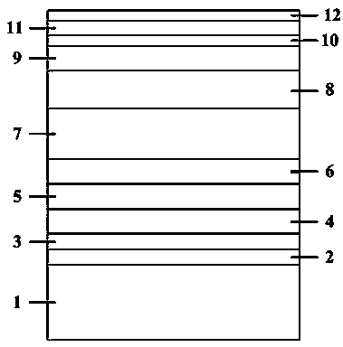
[0039] refer to figure 1 , the growth of microcrack-free Si-based III-nitride epitaxial wafer structures, using the metal-organic chemical vapor deposition (MOCVD) method as an example,

[0040] 1) A 111-sided single-crystal Si with a diameter of 101.6 mm is used as the substrate 1, and the oxide film on the surface of the Si substrate is removed by a hydrofluoric acid-based etching solution before the growth of the nitride epitaxial layer. Then, it is placed in the reaction chamber of the MOCVD apparatus.

[0041] 2) Heating the Si substrate in a hydrogen atmosphere at a pressure of 6.65kPa in the reaction chamber for 1 to 1000 o C, thermal annealing for 10min.

[0042] 3) Keep the reaction chamber pressure constant and lower the substrate temperature to 900 o C, Ammonia gas with a flow rate of 10 L / min and trimethylaluminum (TMA) with a flow rate of 86 μmol / min are injected to grow an AlN nucleation layer 2 with a thickness of 100 nm, and the growth time is 1800 s. Then ...


PUM

PropertyMeasurementUnit
thicknessaaaaaaaaaa

Abstract

The invention discloses a Si (Silicon)-base III nitride epitaxial wafer without microcracks in surface. The Si-base III nitride epitaxial wafer is characterized by comprising an Si substrate, two AlN (aluminium nitride) nucleating layers, three Al<x>Ga<1-x>N intermediate layers with Al components degreased progressively, an AlGa<1-a>N / AlGa<1-b>N superlattice intermediate layer, two GaN channel layers and three barrier layers sequentially from down to up. The Si-base III nitride epitaxial wafer has the advantages that an Si-base III nitride heterojunction is high in surface quality and does not have micro cracks in comparison with an existing technology; furthermore, the AlGaN intermediate layers with progressively-degreased components of which an average Al component is low in an epitaxial layer structure provided by the invention is adopted to achieve an aim of improving surface appearance, therefore, the influence of a pre-reaction between a metal organic source and an ammonia gas can be reduced beneficially, the crystalline quality of the epitaxial wafer can be improved, and the growth rate of the epitaxial wafer can be improved.

Description

technical field [0001] The invention relates to a Si-based Group III nitride epitaxial sheet without microcracks on the surface, in particular to an epitaxial sheet containing a Group III nitride heterojunction capable of generating two-dimensional electron gas. It belongs to the field of semiconductor technology. Background technique [0002] The heterojunction composed of Group III nitride semiconductor materials, such as GaN and Al(In)GaN, can form a two-dimensional electron gas with high concentration and high electron mobility, which is suitable for the development of microwave power field effect transistor devices. Due to the lack of large-sized homogeneous substrates, currently nitride semiconductor materials are mainly grown on substrates such as silicon carbide, sapphire or Si. [0003] Si and III-nitride epitaxial materials have very serious lattice mismatch and thermal mismatch. For example, the thermal mismatch between (0001) plane GaN and (111) plane Si is 54%,...

Claims


Application Information

Patent Timeline
Patent Type & Authority Applications(China)
IPC IPC(8): H01L29/15H01L21/205C30B25/22
CPCC30B25/22C30B29/403H01L21/02381H01L21/0254H01L21/0262
Inventor 倪金玉潘磊
Owner NO 55 INST CHINA ELECTRONIC SCI & TECHNOLOGYGROUP CO LTD
Why Eureka
Try Eureka