Portable low-temperature semiconductor detector device

A detector and semiconductor technology, which is applied in the field of portable low-temperature semiconductor detector devices, can solve problems such as increasing surface leakage current, vibration noise, and poor energy resolution, so as to improve vacuum maintenance time, reduce vibration and noise interference, and reduce Effects of Electronics Noise

Active Publication Date: 2015-02-18
TSINGHUA UNIV +1
View PDF9 Cites 2 Cited by
  • Summary
  • Abstract
  • Description
  • Claims
  • Application Information

AI Technical Summary

Problems solved by technology

However, this design has several defects as follows: (1) The vacuum state of the container will deteriorate or even be destroyed over time, which will lead to two results, namely, (a) impurity molecules or ions in the container It will be adsorbed on the surface of the crystal and destroy the surface state of the crystal, thereby increasing the surface leakage current and reducing the energy spectrum resolution of the detector. The recovery and maintenance process of the surface state is complicated. At present, the imported detectors in China can only do simple vacuum baking. Restoration and maintenance are expensive, for example, ORTEC’s device costs up to 10,000 yuan for one-time vacuum heating treatment; (b) The increase in vacuum breaking pressure causes the convective heat conduction between the detector crystal and the outer wall of the container to increase, and the cooling capacity on the crystal will decrease. It is quickly transferred to the container shell, causing the device shell to sweat or even frost, affecting or even corroding the circuit module near the crystal chamber; (2) the crystal is directly exposed to the vacuum chamber, and the oil vapor volatilized by the vacuum system may affect the crystal. Cause pollution, the consequences are as described in (a) above; (3) The crystal and JFET circuit are in the same chamber, once the vacuum is broken or the electronic accessories are replaced, the crystal will be exposed to the atmosphere, the consequences are as described in (a) above like that
At present, the design of the existing mainstream products is to realize heat conduction between the cold finger of the refrigerator and the crystal through hard connection coupling, the mechanical vibration of the refrigerator will be directly transmitted to the crystal, and the crystal will transmit the vibration to the contact electrode. The charge-sensitive preamplifier of the AC coupling circuit will undoubtedly produce serious vibration noise, which will cause the energy resolution to deteriorate, or even completely submerge the energy spectrum signal. Even for the amplifier of the DC coupling circuit, it will also affect the energy spectrum resolution. Another On the other hand, vibration will form friction between the crystal and the contact electrode to generate static electricity, and static electricity will also bring interference noise

Method used


Image

  • Portable low-temperature semiconductor detector device
  • Portable low-temperature semiconductor detector device

Examples


Embodiment 1

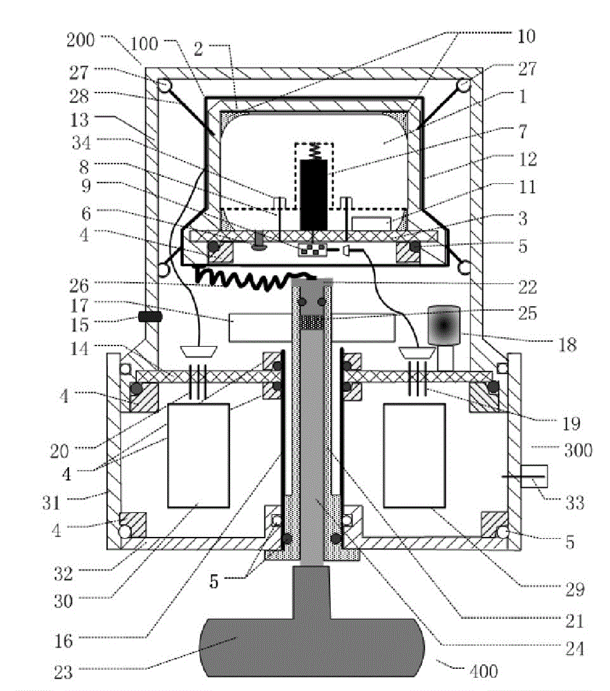
[0117] figure 1 It is a schematic longitudinal sectional view of a portable low-temperature semiconductor detector device according to an embodiment of the present invention. exist figure 1 An embodiment of a portable HPGe detector device is shown in . The device design of this embodiment is suitable for the situation that the electronic system of the detector adopts a DC coupling circuit design: the signal is drawn out from the contact pole on the inner surface of the crystal, and the front circuit is DC coupling. The high-pressure crystal protection chamber 100 for the crystal is directly coupled to the disc-shaped copper seat 22 through the sapphire sheet 25, and the cold finger 24 of the refrigerator and the high-pressure crystal protection chamber 100 for the detector crystal are hard-connected to realize heat conduction.

[0118] The device of the present embodiment includes five major parts: HPGe crystal 1; A high-purity nitrogen high-pressure crystal protection chamb...

Embodiment 2

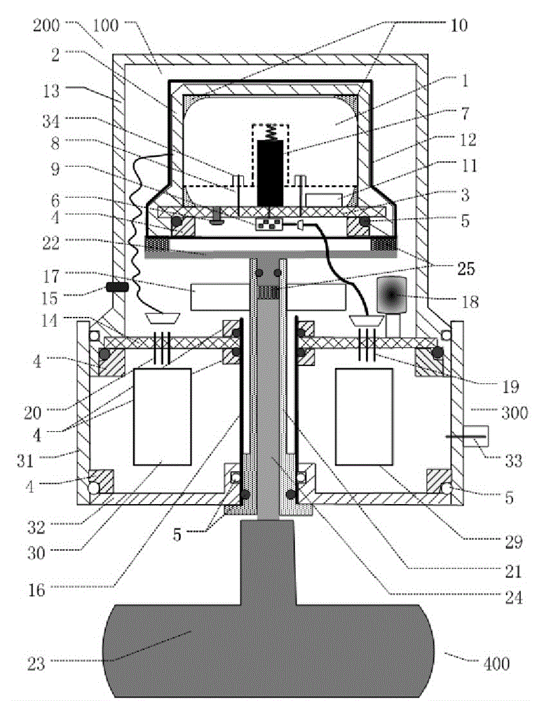
[0132] figure 2 It is a schematic longitudinal sectional view of a portable low-temperature semiconductor detector device according to Embodiment 2 of the present invention. exist figure 2 An embodiment of a portable HPGe detector device is shown in . The device design of this embodiment is suitable for adding high voltage to the contact pole on the inner surface of the crystal and at the same time drawing the signal from the contact pole on the inner surface, and adopts the electronic design of the AC coupling circuit. Consider high-voltage shielding and safe plugging; the disadvantage is that the shock resistance of this circuit is poor, and it is difficult to resist the noise caused by the mechanical vibration of the refrigerator, which affects the resolution of the energy spectrum and even drowns the signal. The invention is implemented according to the principle of vibration reduction of suspension and flexible connection.

[0133] The difference between this embodim...


PUM


Abstract

The invention discloses a portable low-temperature semiconductor detector device which comprises a detector crystal, a high-gas-pressure crystal protection chamber, a vacuum chamber and a refrigerating plant, wherein the high-gas-pressure crystal protection chamber is filled with high-pressure hyperpure inert gases, and the detector crystal is contained in the high-gas-pressure crystal protection chamber; a vacuum environment is formed in the vacuum chamber, and the high-gas-pressure crystal protection chamber is contained in the vacuum chamber; and the refrigerating plant comprises a refrigerating machine and a refrigerating machine cold finger which is connected with the refrigerating machine and is used for cooling the detector crystal.

Description

technical field [0001] The invention relates to a portable low-temperature semiconductor detector device, in particular to a high-purity germanium detector device. Background technique [0002] The band gap of germanium (Ge) semiconductor is very low, so its ionization energy is low (0.09ev). Therefore, detectors made of Ge crystals have two unique advantages: (1) the best energy resolution; (2) High position resolution capability. Therefore, this type of detector is widely used in the measurement of energy spectrum and position information in the fields of high energy physics and nuclear physics. However, due to the low band gap of the semiconductor, the reverse leakage current of the junction field effect transistor (JFET) in the Ge crystal and its electronic system is very large at room temperature, which will directly affect the energy resolution and sensitivity. [0003] The sources of reverse leakage current mainly include surface leakage current, bulk leakage curre...

Claims


Application Information

Patent Timeline
Patent Type & Authority Applications(China)
IPC IPC(8): G01T1/36G01T1/29
Inventor 张清军李元景李玉兰陈志强赵自然刘以农刘耀红马秋峰朱维彬常建平毛绍基何会绍
Owner TSINGHUA UNIV
Why Eureka
Try Eureka