A nano-silicon/silicon nitride film-type electron source and its manufacturing method
A technology of silicon nitride thin film and manufacturing method, which is applied in the manufacture of electrode systems, manufacture of discharge tubes/lamps, circuits, etc., can solve the problem of poor electron emission stability, unstable mechanical and chemical properties of porous silicon electron sources, and unfavorable Preparation of devices for long-term use, etc., to achieve good physical and chemical stability, high melting point and high density, good electron emission ability, and good repeatability
- Summary
- Abstract
- Description
- Claims
- Application Information
AI Technical Summary
Problems solved by technology
Method used
Image

Examples
preparation example Construction
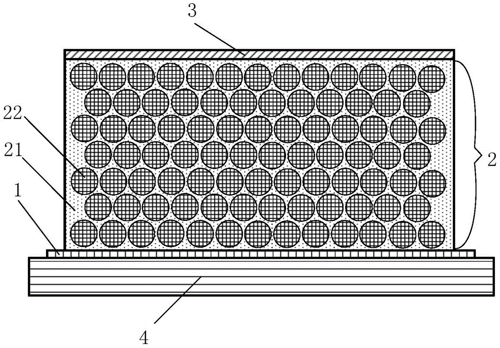
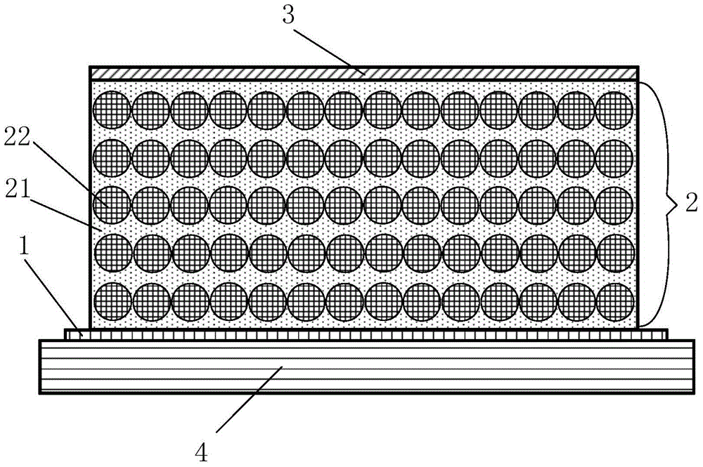
[0036] like figure 1 The preparation method of the first shown nano-silicon / silicon nitride film electron source comprises the following steps:
[0037] 1) Depositing the bottom electrode 1 on the substrate 4 by sputtering a target material of one material among tungsten, nickel, chromium, aluminum, copper, titanium or a composite target material composed of several of them, and its thickness is 40-200nm;
[0038] 2) Depositing a nano-silicon / silicon nitride layer 2 with a thickness of 100-2000nm on the bottom electrode 1, the method is:
[0039] Deposit a silicon-rich silicon nitride film on the bottom electrode 1, in which silicon exists in an amorphous form, and then in nitrogen or a mixed gas composed of nitrogen and hydrogen with a volume ratio of (50:1)-(10:1) Perform high-temperature annealing on the silicon-rich silicon nitride film at 500-1100°C, and the high-temperature annealing time is 30-120 minutes, so that the silicon-rich silicon nitride film (SiN x , x<4 / 3) ...
Embodiment 1
[0062] see figure 1 , the manufacturing process of the nano-silicon / silicon nitride thin film electron source includes the following steps:
[0063] 1) Depositing the bottom electrode 1 on the substrate 4 by using a sputtering tungsten target with a thickness of 200 nm;
[0064] 2) Introduce argon and nitrogen into the coating chamber, control the partial pressure ratio of argon and nitrogen to 3:1, and make the total pressure in the coating chamber 0.1Pa, the temperature of the substrate 4 is controlled at 550°C, and the silicon target Deposit a silicon-rich silicon nitride film with a thickness of 500nm on the bottom electrode 1 as the sputtering source; then, anneal at 900°C for 120 minutes in a mixture of nitrogen and hydrogen with a volume ratio of 25:1 to transform the amorphous silicon into Nanocrystalline silicon 22 to form a silicon nitride 21 film inlaid with nanocrystalline silicon 22, this film is nano-silicon / silicon nitride layer 2, the particle size of silicon ...
Embodiment 2
[0067] see figure 1 , the manufacturing process of the nano-silicon / silicon nitride thin film electron source includes the following steps:
[0068] 1) Depositing the bottom electrode 1 on the substrate 4 by using a sputtering nickel target, the thickness of which is 100 nm;
[0069] 2) Introduce argon gas into the coating chamber, control the air pressure in the coating chamber to 0.3Pa, control the temperature of the substrate 4 at 500°C, and deposit a thickness of 200nm silicon-rich silicon nitride film; then, anneal for 90 minutes at 1000°C in a mixture of nitrogen and hydrogen with a volume ratio of 30:1 to convert amorphous silicon into nanocrystalline silicon 22 to form nanocrystalline silicon embedded 22 silicon nitride 21 film, this film is nano-silicon / silicon nitride layer 2, the particle size of silicon grain 22 is 3-6nm, and the adjacent nano-crystals in the silicon nitride 21 film inlaid with nano-crystal silicon 22 The silicon nitride 21 between the silicon 22...
PUM
| Property | Measurement | Unit |
|---|---|---|
| thickness | aaaaa | aaaaa |
| particle diameter | aaaaa | aaaaa |
| thickness | aaaaa | aaaaa |
Abstract
Description
Claims
Application Information
PatSnap Eureka turns technology decisions into work you can execute. Powered by our Innovation Knowledge Graph, it runs expert workflows across engineering, life sciences, materials and intellectual property. Get your review-ready output in minutes.


