

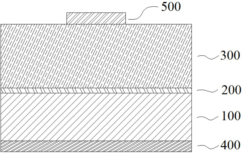
Vertical chip structure for nitride LED (light-emitting diode) and preparation method of vertical chip structure
A chip structure, LED epitaxial wafer technology, applied in semiconductor/solid-state device manufacturing, electrical components, circuits, etc., can solve problems such as absorption loss, and achieve the effects of low cost, high reliability, and simplified process flow
- Summary
- Abstract
- Description
- Claims
- Application Information
AI Technical Summary
Problems solved by technology
Method used
Image

Examples
preparation example Construction
[0097] A method for preparing a nitride LED vertical chip structure, comprising the following steps:
[0098] 1) Fabricate a metal functional film on a conductive substrate to form a composite substrate;
[0099] The preparation method of the metal functional thin film includes at least one of electroplating, chemical plating, ion plating, thermal evaporation, electron beam evaporation and magnetron sputtering;
[0100] Then prepare more than one layer of two-dimensional derived film layers on the composite substrate, that is, prepare more than one layer of graphene or silicene;
[0101] The preparation of the graphene or silicene is grown on the composite substrate by chemical vapor deposition or physical vapor deposition;
[0102] The specific steps for preparing graphene are as follows: the composite substrate is placed in a chemical vapor deposition system, and at a temperature of 400-1050°C, argon and hydrocarbons are introduced simultaneously, and the composite substrat...
Embodiment 1
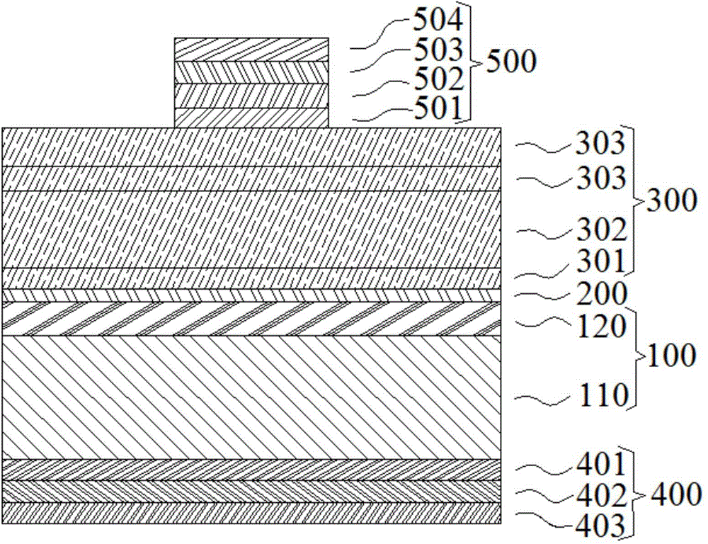
[0120] Such as image 3 As shown, this embodiment shows a schematic structural diagram of a nitride LED vertical chip. in,
[0121] The structure of the nitride LED epitaxial wafer using the composite substrate is as follows from bottom to top: a 2-inch iron-chromium alloy (Fe: 80wt%, Cr: 20wt%) substrate with a thickness of 150 μm constitutes a metal conductive substrate 110; 20nm thick The Ag reflective layer 122 and the 50nm thick Ni catalytic support layer 123 together form a functional metal thin film layer; the multilayer graphene 201 forms a two-dimensional derived film; the buffer layer 301 is composed of 200nm n-type Al 0.1 Ga 0.9 N-layer composition; the structural parameters of the n-type electron injection layer 302 are as follows: a 2 μm thick n-type GaN layer, the doping element is Si, and the doping concentration is 1.0×10 19 ; The structural parameters of the active layer 303 are as follows: In 0.15 Ga 0.85 N / GaN multiple quantum well light-emitting layer,...
Embodiment 2
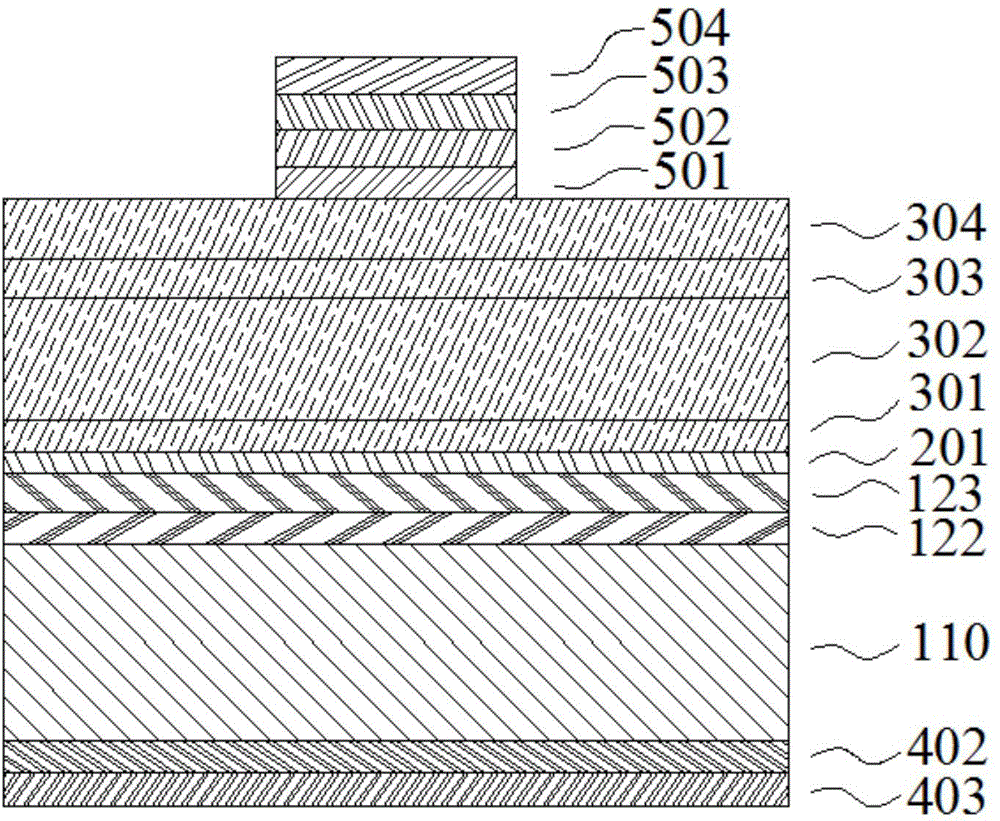
[0131] Such as Figure 4 As shown, this embodiment shows a schematic structural diagram of a nitride LED vertical chip. in,
[0132] The structure of the nitride LED epitaxial wafer using a composite substrate is as follows from bottom to top: a 4-inch size 430 μm thick n-type conductive 6H-SiC substrate constitutes a semiconductor conductive substrate 110; a metal thin film structure Au (200nm) / NiCr (100nm); Wherein, NiCr represents the alloy of Ni and Cr, Ni: 80wt%, Cr: 20wt%) form ohmic contact layer 121; Thickness is that the Ag film of 15nm is reflection layer 122; Thickness is that 40nm Ni film is catalytic supporting layer 123; the ohmic contact layer 121, the reflective layer 122 and the catalytic support layer together form a functional metal thin film layer; the multilayer graphene 201 forms a two-dimensional derived film; the buffer layer 301 is composed of 200nm n-type Al 0.15 Ga 0.85 N-layer composition; the structural parameters of the n-type electron injectio...
PUM
| Property | Measurement | Unit |
|---|---|---|
| thickness | aaaaa | aaaaa |
| thickness | aaaaa | aaaaa |
| thickness | aaaaa | aaaaa |
Abstract
Description
Claims
Application Information