Preparation method of local boron back surface passive field solar cell

A solar cell and back passivation technology, applied in circuits, photovoltaic power generation, electrical components, etc., can solve the problems of increasing the recombination rate of the back side, affecting the photoelectric conversion efficiency of the battery, etc., to improve the photoelectric conversion efficiency, increase the current opening voltage and filling. factor, the effect of increasing the open circuit voltage

Inactive Publication Date: 2015-07-01
JA SOLAR TECH YANGZHOU +1
View PDF3 Cites 18 Cited by
  • Summary
  • Abstract
  • Description
  • Claims
  • Application Information

AI Technical Summary

Problems solved by technology

If the area is too small, it will increase the contact resistance and lateral resistance on the back, if it is too large, it will increase the recombination rate on the back, both of which will affect the photoelectric conversion efficiency of the battery

Method used


Image

  • Preparation method of local boron back surface passive field solar cell
  • Preparation method of local boron back surface passive field solar cell
  • Preparation method of local boron back surface passive field solar cell

Examples


Embodiment 1

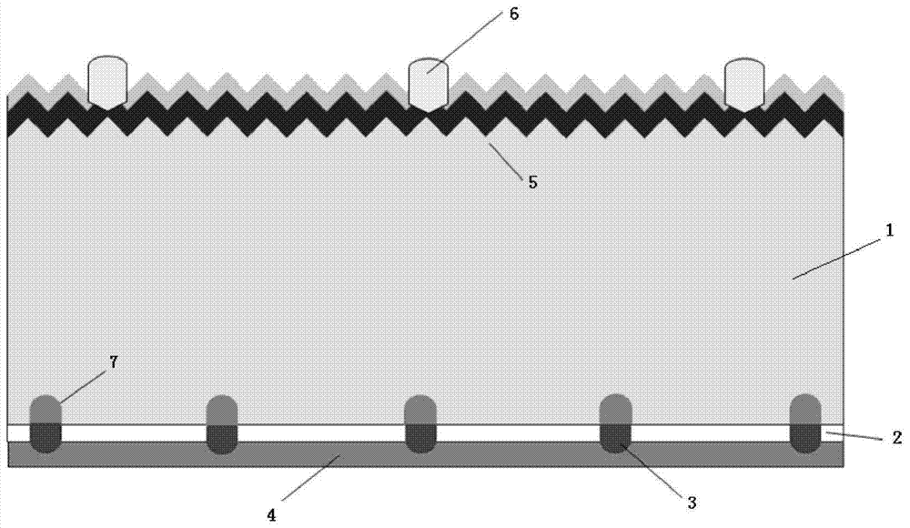
[0045] This embodiment illustrates a method for preparing a partially boron-back field-passivated solar cell. The specific steps of the preparation method are as follows:

[0046] A. Select a p-type monocrystalline silicon wafer 1 with a resistivity of 0.1-10Ω·cm, place it in a texturing tank, and place it in a deionized aqueous solution of sodium hydroxide with a mass percentage of 0.5-5%. Under the condition of 75~90℃, the surface texture is formed to form a suede structure;

[0047] B. Clean the surface of the silicon wafer with a chemical solution. The chemical solution is one or more mixed aqueous solutions of hydrofluoric acid, nitric acid, hydrochloric acid, sulfuric acid and other additives. The cleaning time is 0.5 to 60 minutes and the temperature is 5. ~90°C;

[0048] C. After cleaning the above velvet sheet, place it in a furnace tube at 700-1000° C. to carry out phosphorus (P) diffusion to prepare n-type emitter 5. The diffusion time is 70-150 minutes; the square...

Embodiment 2

[0065] This embodiment illustrates a method for preparing a partially boron-back field-passivated solar cell. The specific steps of the preparation method are as follows:

[0066] A. Select a lightly doped p-type single crystal silicon wafer with a resistivity of 0.1-10Ω·cm, place it in a texturing tank, and put it in a deionized aqueous solution of sodium hydroxide with a mass percentage of 0.5-5%. , at a temperature of 75-90°C, the surface is textured to form a suede structure;

[0067] B. Clean the surface of the silicon wafer with a chemical solution. The chemical solution is one or more mixed aqueous solutions of hydrofluoric acid, nitric acid, hydrochloric acid, sulfuric acid and other additives. The cleaning time is 0.5 to 60 minutes and the temperature is 5. ~90°C;

[0068] C. After cleaning the above textured sheet, place it in a furnace tube at 700-1000°C for phosphorus (P) diffusion to prepare an n-type emitter. The diffusion time is 70-150 minutes, and the square ...

Embodiment 3

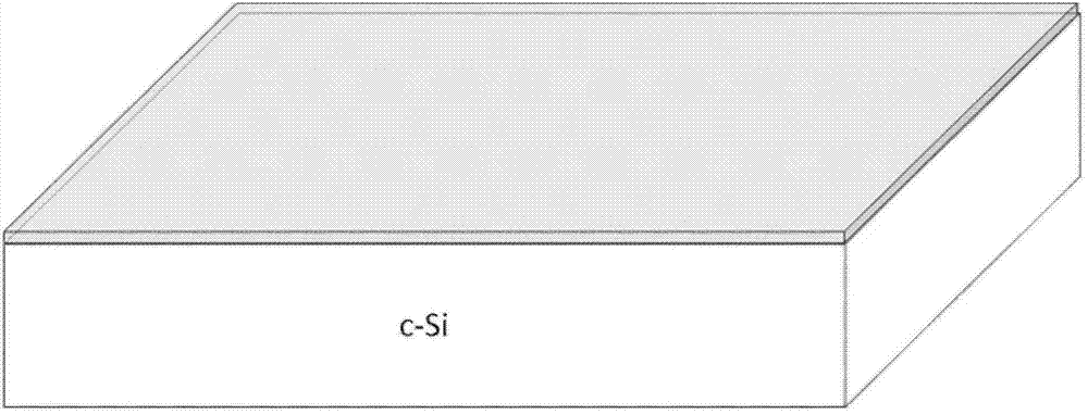
[0085] This embodiment illustrates a method for preparing a partially boron-back field-passivated solar cell. The specific steps of the preparation method are as follows:

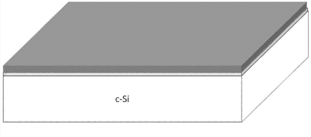
[0086] (1) Select a p-type single crystal silicon wafer, and cover the passivation layer on the back after pretreatment, such as figure 2 As shown in , where the passivation layer is one or both of aluminum oxide and silicon nitride, the pre-treatment includes texturing, cleaning, phosphorus diffusion, removal of back junction and removal of phosphosilicate glass, and the passivation layer is covered on the back Finally, it also includes the process of setting a passivation and anti-reflection layer on the front side of the silicon wafer;

[0087] (2) The boron source is completely covered on the passivation layer, such as image 3 As shown in , the boron source is a boron-containing slurry. The boron slurry generally contains boron-containing compounds such as boron oxide or other boron-doped media such ...


PUM

PropertyMeasurementUnit
thicknessaaaaaaaaaa
diameteraaaaaaaaaa
lengthaaaaaaaaaa

Abstract

The invention discloses a preparation method of a local boron back surface passive field solar cell. The preparation method of the local boron back surface passive field solar cell includes following steps: (1) selecting a p type single crystal silicon wafer, and covering the back surface of the p type single crystal silicon wafer with a passive layer after pretreatment; (2) arranging a boron source on the passive layer; (3) using a laser to enable the boron source to penetrate through the passive layer, and then mingling the boron source into a silicon substrate so as to generate local boron doping; (4) arranging sizing containing silver above a local boron doping area; (5) completely covering the back surface of the p type single crystal silicon wafer with an aluminum layer, and obtaining the local boron back surface passive field solar cell through subsequent processing. The preparation method of the local boron back surface passive field solar cell can decrease the back metallization contact area, reduces back surface recombination, lateral resistance and contact resistance, increases electric current opening voltage and fill factors of the local boron back surface passive field solar cell and components, and improves photoelectric conversion efficiency of the local boron back surface passive field solar cell and the components.

Description

technical field [0001] The invention belongs to the technical field of photovoltaics, and in particular relates to a preparation method of a partial boron back passivation solar cell. Background technique [0002] Photovoltaic technology is a technology that uses large-area p-n junction diodes to convert solar energy into electrical energy. This p-n junction diode is called a solar cell. The semiconductor materials used to make solar cells have a certain band gap. When the solar cell is irradiated by the sun, photons with energy exceeding the band gap generate electron-hole pairs in the solar cell. The p-n junction separates the electron-hole pairs, and the p-n junction The asymmetry determines the flow direction of different types of photo-generated carriers, and the external power can be output through the external circuit connection. This is similar to the principle of ordinary electrochemical cells. [0003] Industrial production of p-type crystalline silicon solar ce...

Claims


Application Information

Patent Timeline
Patent Type & Authority Applications(China)
IPC IPC(8): H01L31/18H01L31/0224
CPCH01L31/022441H01L31/1804Y02E10/547Y02P70/50
Inventor 蒋秀林吴兰峰刘志锋单伟
Owner JA SOLAR TECH YANGZHOU
Why Eureka
Try Eureka