
Light-emitting diode structure with indium-containing conductive layer and preparation method therefor

A technology of light-emitting diodes and conductive layers, applied in circuits, electrical components, semiconductor devices, etc., can solve the problems of poor InGaN quantum well crystal quality, large lattice mismatch, low internal quantum efficiency, etc., to improve spontaneous radiation recombination. rate, improve crystal quality, improve the effect of crystal quality

Inactive Publication Date: 2015-10-14
SOUTH CHINA UNIV OF TECH
View PDF4 Cites 3 Cited by
  • Summary
  • Abstract
  • Description
  • Claims
  • Application Information

AI Technical Summary

Problems solved by technology

[0007] The present invention aims at the problems of low internal quantum efficiency caused by the large mismatch between the InGaN well and the GaN lattice of the existing GaN-based light-emitting diode epitaxial wafer, the poor crystal quality of the InGaN quantum well, and the serious separation of the electron-hole wave function. N-type InGaN as N-type conductive layer, unintentionally doped InGaN as multi-quantum well barrier layer, and P-type InGaN as P-type conductive layer Light-emitting diode structure with indium-containing conductive layer and preparation method thereof

Method used


Image

  • Light-emitting diode structure with indium-containing conductive layer and preparation method therefor
  • Light-emitting diode structure with indium-containing conductive layer and preparation method therefor
  • Light-emitting diode structure with indium-containing conductive layer and preparation method therefor

Examples


Embodiment 1

[0041] Example 1 , A light-emitting diode epitaxial structure with n-type and p-type InGaN conductive layers

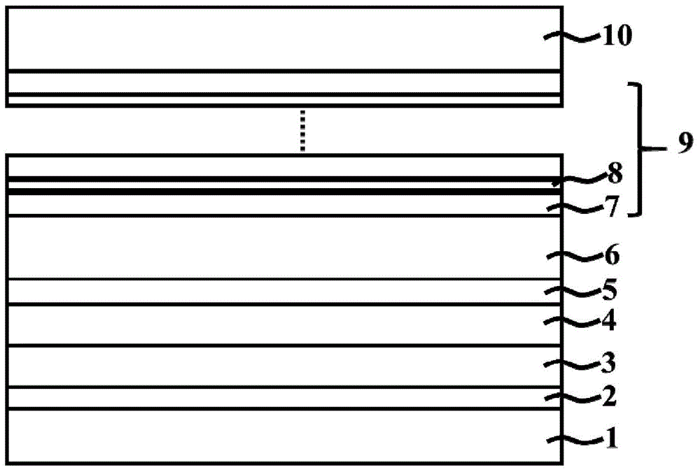
[0042] Such as figure 1 As shown, the light-emitting diodes are sapphire substrate 1, GaN nucleation layer 2, unintentionally doped GaN layer 3, N-type GaN conductive layer 4, In composition graded InGaN layer 5, N-type InGaN layer from bottom to top. Conductive layer 6, multi-quantum well active region 9 and P-type InGaN conductive layer 10.

[0043] The epitaxial growth steps are as follows:

[0044] (1). Put the sapphire substrate into the metal-organic chemical vapor phase chemical deposition equipment, pass in hydrogen, raise the temperature of the reaction chamber to 1300 degrees Celsius, and perform high-temperature cleaning on the substrate.

[0045] (2). The temperature is lowered to 550 degrees Celsius, and the reaction chamber is filled with ammonia gas, hydrogen gas and trimethylgallium, and a 30 nm GaN nucleation layer is grown on the substrate descri...

Embodiment 2

[0056] Example 2 , A light-emitting diode epitaxial structure with n-type and p-type InGaN conductive layers

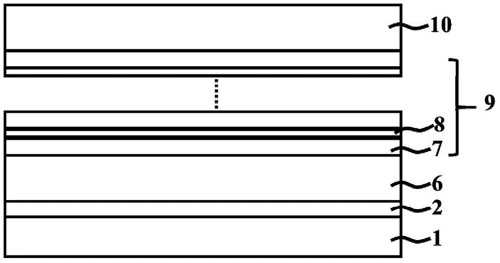
[0057] Such as figure 2 As shown, the light-emitting diode is sequentially composed of a sapphire substrate 1, a GaN nucleation layer 2, an N-type InGaN conductive layer 6, a multi-quantum well active region 9, and a P-type InGaN conductive layer 10 from bottom to top. The preparation method is as follows: As in Example 1, the difference is:

[0058] After the growth on the nucleation layer described in step (2) is completed, directly enter step (6), the reaction chamber is fed with silane, ammonia, hydrogen trimethylgallium and trimethylindium, and the temperature is kept at 800 degrees Celsius. ) on the sample described above, grow an N-type doped InGaN conductive layer with a thickness of 2.5 um and a doping concentration of 8×10 18 cm -3 .

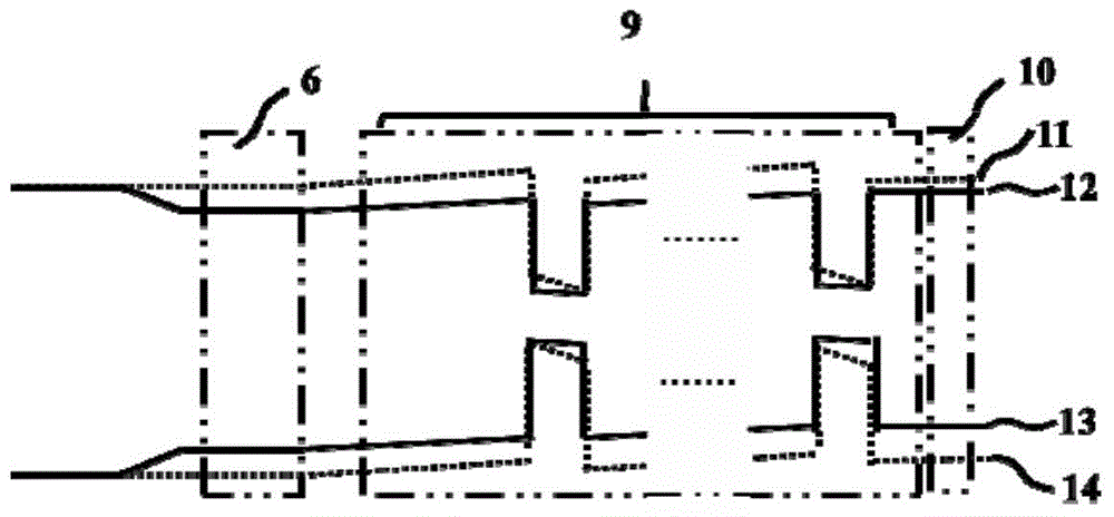
[0059] Depend on image 3 It can be seen that the figure includes a P-type InGaN conductive layer 10; a conduction b...


PUM

PropertyMeasurementUnit
Thicknessaaaaaaaaaa
Thicknessaaaaaaaaaa
Thicknessaaaaaaaaaa

Abstract

The invention relates to a light-emitting diode structure with an indium-containing conductive layer and a preparation method therefor. The light-emitting diode structure comprises a sapphire substrate, a GaN nucleating layer, an unintentional GaN-doped layer, an N type GaN conductive layer, an In component gradient change layer, an N type InGaN conductive layer, a multi-quantum-well active region and a P type InGaN conductive layer. According to the light-emitting diode structure, InGaN is used for replacing traditional GaN to be used as N type and P type conducive layers so that the metal-GaN contact barrier height can be greatly reduced, the working voltage of a GaN-based LED is reduced and the luminous efficiency of the GaN-based LED is improved. Furthermore, the InGaN is used as the N type conductive layer and a quantum well barrier layer so that the lattice constant of the barrier layer is closer to the lattice constant of a potential well layer; the lattice mismatch degree is reduced and the crystal mass of quantum wells can be improved; and the polarization charge density on the two sides of the quantum wells is reduced and the inner quantum efficiency of the GaN-based LED is improved.

Description

technical field [0001] The invention relates to the technical field of light-emitting diodes, in particular to a light-emitting diode structure with an indium-containing conductive layer and a preparation method thereof. Background technique [0002] A light-emitting diode (referred to as "LED") is a semiconductor solid-state light-emitting device. It uses the conduction band electrons and valence band holes inside the semiconductor material to undergo radiative recombination, and releases energy in the form of photons to directly emit light. By designing different bandgap widths of semiconductor materials, light-emitting diodes can emit light in different bands from infrared to ultraviolet. [0003] Nitride light-emitting diodes have been widely developed around the world due to their advantages of high efficiency, energy saving, long life and small size. Ultraviolet light-emitting diodes with a luminous wavelength of 210-365nm have broad application prospects in the field...

Claims


Application Information

Patent Timeline
IPC IPC(8): H01L33/32H01L33/06
CPCH01L33/32H01L33/06H01L33/325
Inventor 徐明升王洪周泉斌
Owner SOUTH CHINA UNIV OF TECH
Features
  • Generate Ideas
  • Intellectual Property
  • Life Sciences
  • Materials
  • Tech Scout
  • Unparalleled Data Quality
  • Higher Quality Content
  • 60% Fewer Hallucinations
Learn More