
Polycrystalline silicon wafer texturing auxiliary and application method thereof

A polycrystalline silicon wafer and application method technology, applied in the field of solar cells, can solve problems such as difficulty in adapting to polycrystalline silicon wafers, sensitive surface conditions of silicon wafers, large equipment investment, etc., so as to improve experimental repeatability, improve texturing uniformity, and improve texturing. The effect of surface uniformity

Inactive Publication Date: 2016-02-03
SUZHOU SOLARING TECH
View PDF12 Cites 19 Cited by
  • Summary
  • Abstract
  • Description
  • Claims
  • Application Information

AI Technical Summary

Problems solved by technology

[0002] Due to the existence of grains with multiple orientations on polycrystalline silicon wafers, isotropic acid etching is generally used to prepare the textured surface to reduce the surface reflectivity, but there are three problems in this method: 1) The surface reflectivity of the silicon wafer after texture is high, and the reflection The corrosion rate is generally above 20%, which severely restricts the photoelectric conversion efficiency of polycrystalline silicon solar cells; 2) The reaction solution needs to be cooled to below 10°C during the texturing process. Since the corrosion reaction is a violent exothermic reaction, the energy consumption of this method is very large ; 3) This texturing method is only suitable for polysilicon wafers obtained by mortar cutting, and diamond wire cutting is a more economical and environmentally friendly method, which is bound to replace the traditional mortar cutting method. There are few and shallow cutting defects on the surface of polysilicon wafers, and the traditional acid etching method cannot obtain a surface with qualified reflectivity. It is for this reason that diamond wire-cut polysilicon wafers have not been widely used in cell manufacturers
[0003] Patent CN101800264A mentions the method of preparing polysilicon textured surface by dry plasma etching. Although a lower surface reflectivity can be obtained, the surface of the silicon wafer is easily damaged by plasma bombardment, and subsequent treatment is required. Otherwise, the surface of the silicon wafer will be seriously compounded and cannot Obtain high-efficiency solar cells. In addition, the equipment investment of this method is large, and the utilization rate of the reaction gas raw materials is low due to vacuuming. The main gas raw materials are fluoride or sulfide, which are highly toxic gases.
[0004] Patents CN103456804A and CN102051618A mention the use of metal-induced corrosion to prepare textured surfaces. This method utilizes the catalytic action of metal ions to prepare nanowire structures or nanohole structures with low reflectivity on the surface of silicon wafers. This method exists as follows Problems: 1) This method is an anisotropic etching method, and it is very sensitive to the surface conditions of silicon wafers, so it is difficult to adapt to polycrystalline silicon wafers cut by diamond wire; "Raindrop" traces are left on the surface, which affects the appearance uniformity of the silicon wafer surface; 3) Due to factors such as pH value, the experimental repeatability of this method is not good; 4) The characteristic size of the prepared textured structure is often only a few Nanometer or dozens of nanometers, the surface area is huge, and effective surface passivation cannot be implemented in the follow-up, resulting in very serious surface recombination, which makes the photoelectric conversion efficiency of the prepared solar cell low
Since the chemical components in the texturing liquid are volatile at room temperature, these components will volatilize faster at high temperatures, making it difficult to control the composition ratio of the texturing liquid

Method used


Image

  • Polycrystalline silicon wafer texturing auxiliary and application method thereof
  • Polycrystalline silicon wafer texturing auxiliary and application method thereof
  • Polycrystalline silicon wafer texturing auxiliary and application method thereof

Examples


Embodiment 1

[0039] 1) Configure the texturing liquid: the proportion and method are the same as in Comparative Example 1.

[0040] 2) Prepare auxiliary agent: Add 10% hydrogen peroxide by volume, 0.1mol / L silver nitrate, 1% ammonium fluoride by mass and 100ppm ethylene glycol in deionized water in sequence, and stir evenly to prepare auxiliary agent .

[0041] 3) Texturing: Add 1% volume ratio auxiliary agent to the texturing liquid and stir evenly, immerse the polysilicon wafer cut by the mortar into the texturing liquid, control the temperature at 30°C, and the reaction time is 240s. After the reaction was completed, the silicon wafer was immersed in an aqueous sodium hydroxide solution with a temperature of 25°C and a mass concentration of 0.5% to remove the porous structure on the surface for 180 s.

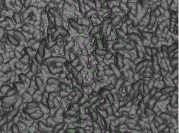
[0042]After the texturing is completed, the silicon wafer is cleaned and dried, and its surface reflectance is measured to be about 8%. The photo of its surface morphology is as follows...

Embodiment 2

[0044] 1) Configure the texturing liquid: the proportioning and method are the same as in Comparative Example 1.

[0045] 2) Preparation of auxiliary agents: Add 15% volume ratio of hydrogen peroxide, 0.2mol / L silver nitrate, 1% mass ratio of ammonium bifluoride and 100ppm ethylene glycol in deionized water in sequence, and stir evenly to prepare auxiliary agents.

[0046] 3) Texturing: add 2% volume ratio of auxiliary agent to the texturing liquid and stir evenly, immerse the diamond wire-cut polysilicon wafer in the texturing liquid, the temperature is controlled at 40°C, and the reaction time is 300s. After the reaction was completed, the silicon wafer was immersed in a sodium hydroxide solution with a temperature of 25 °C and a mass concentration of 1% to remove the porous structure on the surface for 240 s.

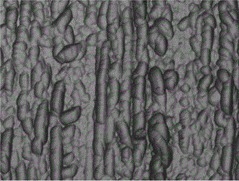
[0047] After the texturing is completed, the silicon wafer is cleaned and dried, and its surface reflectance is measured to be about 15%, and its appearance is as fo...


PUM


Abstract

The invention provides a polycrystalline silicon wafer texturing auxiliary and an application method thereof. The auxiliary comprises a silver inducer, an oxidizing agent, a buffering agent, a dispersing agent and deionized water. The auxiliary is added to a traditional isotropic texturing liquid composed of mixed liquor of hydrofluoric acid and nitric acid, then a polycrystalline silicon wafer is immersed in the texturing liquid, and isotropic corrosion and anisotropic corrosion occur on the surface of the silicon wafer, thereby obtaining a silicon surface with coexisting isoropic corrosion pits whose reflectivity is lower than 10% and anisotropic inverted pyramid morphology. The function of the buffering agent is to maintain the stability of a PH value of the texturing liquid; the oxidizing agent can suppress anisotropic corrosion of the silver inducer, thereby avoiding formation of too deep holes; and the dispersing agent can avoid the ''raindrop'' defect, and also wraps nano-silver particles attached to the surface of the silicon wafer, thereby substantially reducing cleaning difficulty of the silicon wafer after texturing. The polycrystalline silicon wafer texturing auxiliary provided by the invention overcomes some deficiencies of existing polycrystalline silicon texturing methods, and is particularly suitable for texturing of a polycrystalline silicon wafer cut by diamond wires.

Description

technical field [0001] The invention relates to the technical field of solar cells, in particular to a polycrystalline silicon wafer texturing auxiliary agent and an application method thereof. Background technique [0002] Due to the existence of grains with multiple orientations on polycrystalline silicon wafers, isotropic acid etching is generally used to prepare the textured surface to reduce the surface reflectivity, but there are three problems in this method: 1) The surface reflectivity of the silicon wafer after texture is high, and the reflection The corrosion rate is generally above 20%, which severely restricts the photoelectric conversion efficiency of polycrystalline silicon solar cells; 2) The reaction solution needs to be cooled to below 10°C during the texturing process. Since the corrosion reaction is a violent exothermic reaction, the energy consumption of this method is very large ; 3) This texturing method is only suitable for polysilicon wafers obtaine...

Claims


Application Information

Patent Timeline
IPC IPC(8): H01L31/0236C30B33/10C30B29/06
Inventor 刘锋季根华李翔
Owner SUZHOU SOLARING TECH
Learn More