Si-containing nanometer porous Pd material and preparation method thereof
A nano-porous, high-content technology, which is applied in the direction of electrical components, circuits, battery electrodes, etc., can solve the problems that hinder the practical application of nano-porous materials, the difficulty of testing related properties of nano-porous structures, and fragility, and achieve uniform pore size. control, excellent catalytic performance, and good structural integrity
- Summary
- Abstract
- Description
- Claims
- Application Information
AI Technical Summary
Problems solved by technology
Method used
Image
Examples
preparation example Construction
[0017] The first is the preparation of precursor alloy strip samples, which includes three steps: raw material proportion weighing, alloy ingot melting and strip sample preparation. The specific operation is as follows:
[0018] Step 1: Raw material ratio weighing
[0019] According to the chemical composition of the material Cu 1-x-y PD x Si y (10% ≤ x ≤ 30%, 0% < y ≤ 10%), select a suitable proportion of ingredients, convert according to the proportion and weigh the weight of each component raw material, ready to use. The purity of the metal raw materials used is: 99.99wt.% Cu, 99.5wt.% Pd and 99.999wt.% Si.
[0020] Step 2: Alloy ingot melting
[0021] The weighed raw materials of each component are mixed, placed in a water-cooled copper crucible of a non-consumable arc melting furnace, and smelted under the protection of high-purity argon, and the smelting is repeated three times to obtain an alloy ingot with a relatively uniform composition. The alloy mass loss rate...
Embodiment 1
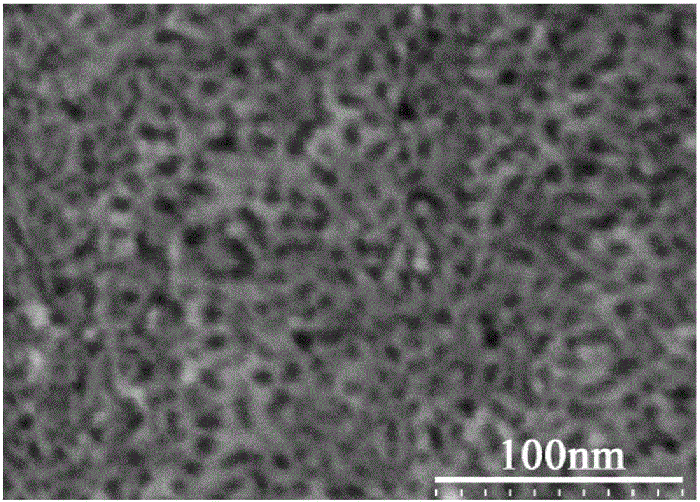
[0040] Example 1Cu 75 PD 20 Si 5 alloy
[0041] Step 1: Weighing of component materials and melting of alloy ingot
[0042] Will Cu 75 PD 20 Si 5 The atomic percentage is converted into weight percentage, the ingredients are weighed, the weighed raw materials are mixed, placed in the water-cooled copper crucible of the non-consumable arc melting furnace, and arc melting is carried out under the protection of high-purity argon, and then the The alloy ingot is flipped up and down, and smelted repeatedly 3 times to obtain an alloy ingot with uniform composition.
[0043] Step 2: Preparation of strip samples
[0044] The alloy ingot obtained by smelting is crushed, put into a quartz tube with a nozzle size of 8 mm long × 1 mm wide, and then the quartz tube is placed in an induction heating coil for heating, and the molten alloy is blown out with high-purity argon to make it Spray on a high-speed rotating water-cooled copper roller with a linear speed of 40m / s to obtain all...
Embodiment 2
[0054] Example 2Cu 75 PD 24 Si 1 alloy
[0055] Step 1: Weighing of component materials and melting of alloy ingot
[0056] Same as Step 1 in Example 1.
[0057] Step 2: Preparation of strip samples
[0058] Same as Step 2 in Example 1.
[0059] Step 3: Analysis of the structure of the precursor alloy
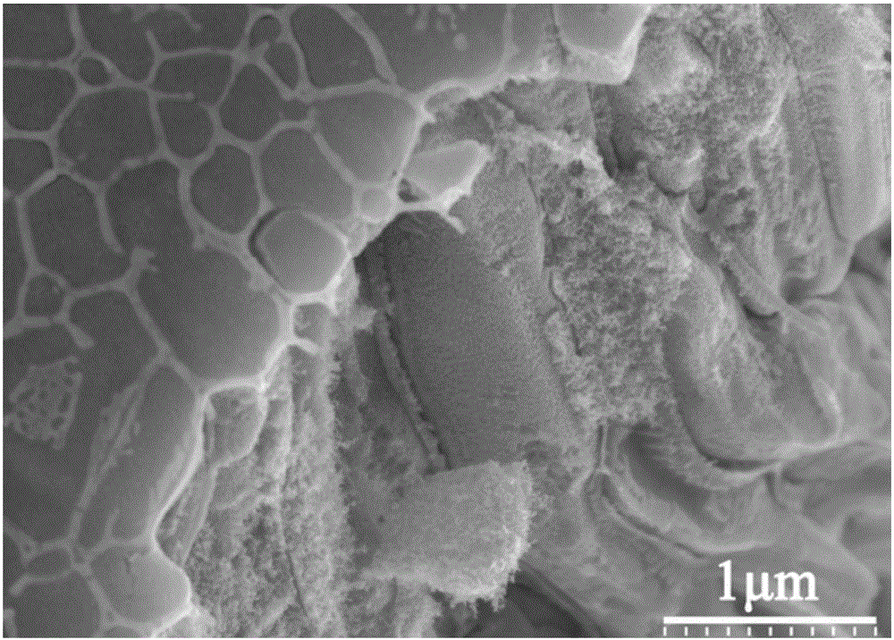
[0060] With step 3 in embodiment 1, analysis result shows that Cu 75 PD 24 Si 1 The alloy is a nearly single FCC solid solution structure, the grain size is about 0.5-4μm, and there are very few Si-rich precipitates on the grain boundaries.
[0061] Step 4: Electrochemical performance test and dealloying experiment
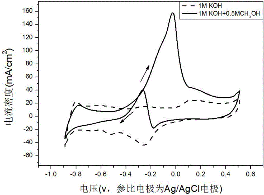
[0062] Using Gamry Interface 1000 electrochemical workstation, in 0.5mol / L H 2 SO 4 solution, for Cu 75 PD 24 Si 1 The room temperature electrochemical performance evaluation of alloy strips (scanning rate is 1mV / s), the measured critical potential is about 1.4V (experimental reference electrode is Ag / AgCl electrode, the same below), which is higher ...
PUM
| Property | Measurement | Unit |
|---|---|---|
| Size | aaaaa | aaaaa |
| Size | aaaaa | aaaaa |
| Grain size | aaaaa | aaaaa |
Abstract
Description
Claims
Application Information


