Single selenium micron tube photoelectric detector, and preparation method and responsivity reinforcement method therefor
A technology of photodetectors and microtubes, applied in semiconductor/solid-state device manufacturing, circuits, nanotechnology, etc., can solve the problems of low responsivity of selenium photodetectors, and achieve good universality, good adhesion, and light response The effect of increasing
- Summary
- Abstract
- Description
- Claims
- Application Information
AI Technical Summary
Problems solved by technology
Method used
Image

Examples
Embodiment 1
[0037] Embodiment 1, the synthesis of selenium microtube
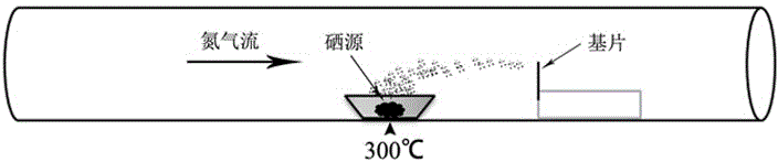
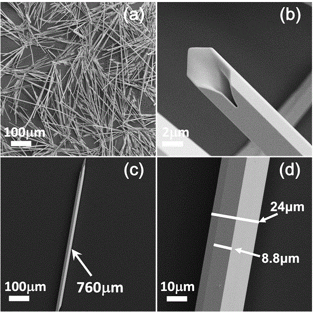
[0038] Take 1g of selenium powder with a purity of 99.95% in a quartz boat and place it in the center of a 1m tube furnace, and place clean SiO2 vertically at a distance of 25cm from the selenium powder 2 / Si substrate. N at 300 sccm flow rate 2 Under these conditions, the central temperature of the tube furnace was heated from room temperature to 300 °C within 55 min, and kept at this temperature for 720 min. N during heat preservation 2 Always maintain a constant rate of flow from Se source to SiO 2 / Si substrate to transfer the evaporated selenium vapor to the growth substrate. After the heat preservation is completed, the core temperature is naturally cooled from the highest temperature to room temperature. SiO 2 / Si substrate is taken out, and selenium microtubes with good crystallinity can be obtained on the surface of the substrate.
[0039]Repeat the above steps, the SiO 2 The / Si substrate is placed 28...
Embodiment 2
[0044] Embodiment 2, preparation of Au nanoparticles
[0045] The prepared selenium microtube detector was placed in the cavity of the ion sputtering apparatus, and the vacuum was evacuated to 0.15 mbar, and kept at this vacuum degree. Then the sputtering current was adjusted to 2 mA, and the sputtering time was set to 150 s. In an air atmosphere, the air plasma in the ion sputterer hits the gold target and transfers the gold atoms to the surface of the selenium microtubes. After sputtering is complete, stop vacuuming and slowly increase the pressure of the chamber to normal pressure. Then it was annealed in an oven at 90 °C under air condition for 3 min, so that the above-mentioned Au films were agglomerated to form Au nanoparticles. After the annealing was completed, the device was naturally cooled to room temperature.
[0046] Repeat the above operation steps, adjust the vacuum degree in the sputtering chamber to 0.1 mbar, adjust the sputtering time to 210s, and a simila...
Embodiment 3
[0049] Embodiment 3, photoelectric performance test of selenium microtube
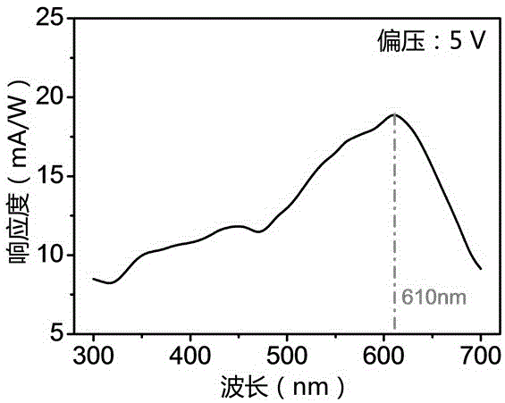
[0050] On the basis of the prepared selenium microtubes, a single microtube is transferred to a glass substrate, and In electrodes are respectively pressed on both ends to form a photodetector with a "metal electrode-semiconductor-metal electrode" structure. Then through the photoelectric test system, under the condition of 5V bias and no light, the dark current of the device is about 60 pA, and the photocurrent of the device is 1.66 nA, 2.53 nA, 1.78 nA, both increased by about 30 times. Under the irradiation of pulsed laser, the rising and falling speeds are 0.32 ms and 23.02 ms, respectively. In addition, the device has good responsivity between 300 and 700 nm, and the highest responsivity is at 610 nm, according to the formula: R λ =(I light - I dark ) / P λ S ( I light : photocurrent I dark : dark current, P λ : wavelength-specific optical power density, S : effective illuminatio...
PUM
| Property | Measurement | Unit |
|---|---|---|
| length | aaaaa | aaaaa |
| width | aaaaa | aaaaa |
Abstract
Description
Claims
Application Information
 - R&D
- Intellectual Property
- Life Sciences
- Materials
- Tech Scout
- Unparalleled Data Quality
- Higher Quality Content
- 60% Fewer Hallucinations
Browse by: Latest US Patents, China's latest patents, Technical Efficacy Thesaurus, Application Domain, Technology Topic, Popular Technical Reports.
© 2025 PatSnap. All rights reserved.Legal|Privacy policy|Modern Slavery Act Transparency Statement|Sitemap|About US| Contact US: help@patsnap.com