Method for preparing barium titanate nanometer ferroelectric film based on pulsed electron beam deposition technology

A technology of pulsed electron beam and barium titanate, which is applied in the field of microelectronics to achieve the effect of low requirements, reduced production cost and good compactness

Active Publication Date: 2019-07-09
NANJING UNIV OF AERONAUTICS & ASTRONAUTICS
View PDF3 Cites 0 Cited by
  • Summary
  • Abstract
  • Description
  • Claims
  • Application Information

AI Technical Summary

Problems solved by technology

At present, the method of depositing barium titanate nanoscale ferroelectric thin film by pulsed electron beam deposition system has not been reported yet.

Method used


Image

  • Method for preparing barium titanate nanometer ferroelectric film based on pulsed electron beam deposition technology
  • Method for preparing barium titanate nanometer ferroelectric film based on pulsed electron beam deposition technology
  • Method for preparing barium titanate nanometer ferroelectric film based on pulsed electron beam deposition technology

Examples


Embodiment 1

[0050] Take a four-inch silicon wafer and cut it into a size of 1cm*1cm, put it in acetone, isopropanol, and ethanol for 15 minutes respectively (ultrasonic power 300W), and then dry it with nitrogen. The cleaned silicon wafer is placed in the pulse e-book deposition chamber, fixed with the substrate with silver glue, and the growth of barium titanate nano-ferroelectric thin film is carried out. The specific steps are as follows:

[0051]1) Clean up the reaction chamber pollutants:

[0052] Put the barium titanate target and the target substrate into the reaction chamber of the pulsed electron beam deposition system, and evacuate the chamber at a molecular pump speed of 1000 Hz until the vacuum degree reaches 1.0×10 -6 Torr or below;

[0053] 2) Control the partial pressure of oxygen in the reaction chamber:

[0054] Slow down the molecular pump to keep it at 250 Hz, then fill the chamber with oxygen to keep the chamber pressure at 6×10 -3 Torr;

[0055] 3) Growth of bariu...

Embodiment 2

[0067] A four-inch silicon wafer was cut into a size of 1 cm*1 cm, and placed in acetone, isopropanol, and ethanol for ultrasonic cleaning (ultrasonic power 300W) for 15 minutes each, and then dried with nitrogen. The cleaned silicon wafer is placed in the pulse e-book deposition chamber, fixed with the substrate with silver glue, and the barium titanate nano-ferroelectric film is grown, except for step 3) to grow the barium titanate film, the target temperature is 500 ℃, The heating rate is 5-20°C / min, and the rest of the steps are the same as in Example 1.

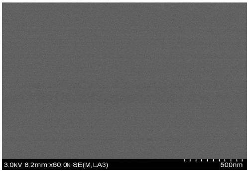
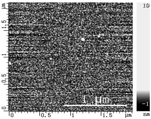
[0068] The barium titanate nano ferroelectric thin film obtained in this embodiment is characterized and tested:

[0069] Figure 6 The image of the surface of the barium titanate nanoferroelectric thin film obtained for this example under a scanning electron microscope shows that the surface of the thin film is relatively smooth.

[0070] Figure 7 The image of the surface of the barium titanate nanoferroelectric thi...

Embodiment 3

[0073] Cut a four-inch silicon wafer into a size of 1 cm*1 cm, and place it in acetone, isopropanol, and ethanol for ultrasonic cleaning (ultrasonic power 300W) for 15 minutes each, and then dry it with nitrogen. The silicon wafer after cleaning is placed in the deposition chamber of the pulse e-book, and it is fixed with the substrate with silver glue, and the growth of barium titanate nano-ferroelectric thin film is carried out, except in step 3) in the growth of barium titanate thin film, the electron gun voltage is set as 10 KV, the number of pulses is 13000, the frequency is 5Hz, and the rest of the steps are the same as in Example 1.

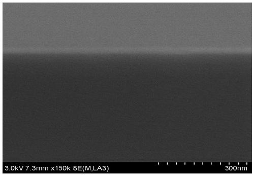
[0074] The barium titanate nano ferroelectric thin film obtained in this embodiment is characterized and tested:

[0075] Figure 9 The image of the surface of the barium titanate nano ferroelectric film obtained for this example under a scanning electron microscope shows that there are obvious crystal grains on the surface of the film, w...


PUM

PropertyMeasurementUnit
thicknessaaaaaaaaaa
electrical resistivityaaaaaaaaaa

Abstract

The invention discloses a method for preparing a barium-titanate ferroelectric nano-film based on a pulsed electron beam deposition technology. The method comprises the following specific steps that firstly, a target substrate and pollution substances in a reaction chamber are cleaned; then partial pressure of oxygen in the reaction chamber is controlled and a barium titanate film grows; and finally in situ annealing is carried out on the barium titanate film to obtain the barium-titanate ferroelectric nano-film. According to the method, the surface of a barium titanate target material is bombarded by a pulsed electron beam generated by an electric spark tunnel system, the energy of the electron beam absorbed by the target material is converted into heat energy to volatilize the material, the volatilized material and plasma formed by ionization are diffused above the surface of the barium titanate target material and then reach the surface of the target substrate, so that the film is formed; and the deposition speed and the thickness of the barium titanate film are further controlled by controlling the pulse number and the pulse frequency of the electron beam, and therefore the prepared barium titanate film is good in compactness and smooth in surface, and the quality of the device is improved.

Description

technical field [0001] The invention belongs to the technical field of microelectronics, and in particular relates to a preparation method of barium titanate nanometer ferroelectric film, which can be used in the preparation of ferroelectric film and semiconductor devices. Background technique [0002] Ferroelectric materials are a class of functional materials with properties such as ferroelectricity, piezoelectricity, high dielectric constant, and photoelectricity. Ferroelectric thin film is a thin film grown on a specific substrate such as metal, semiconductor or insulator with a thickness ranging from tens of nanometers to tens of microns, which can be well combined with micro-nano systems to reduce device size and achieve specific functional application. Ferroelectric thin films have developed into a kind of thin film materials commonly used in microelectronic devices and optical devices, and have attractive applications in the fields of home appliances, communications...

Claims


Application Information

Patent Timeline
Patent Type & Authority Patents(China)
IPC IPC(8): C23C14/08C23C14/30C23C14/58
CPCC23C14/088C23C14/30C23C14/5806
Inventor 郭万林陈红烨邱婷婷王辽宇周建新
Owner NANJING UNIV OF AERONAUTICS & ASTRONAUTICS
Why Eureka
Try Eureka