Formation method for germanium-doped SiC ohmic contact

An ohmic contact and silicon carbide technology, applied in semiconductor devices, electrical components, circuits, etc., can solve the problems of inability to improve the actual effect of ohmic contact and low contact resistance, and achieve the effect of passivation and oxidation tendency and reducing contact resistance.

Inactive Publication Date: 2017-09-01
SHANDONG UNIV +2
View PDF13 Cites 6 Cited by
  • Summary
  • Abstract
  • Description
  • Claims
  • Application Information

AI Technical Summary

Problems solved by technology

This method forms n-type and p-type ohmic contacts at the same time. Although the process steps are reduced, the actual effect of ohmic contacts cannot be improved, and high-performance ohmic contacts with high quality and low contact resistance are formed.

Method used


Image

  • Formation method for germanium-doped SiC ohmic contact
  • Formation method for germanium-doped SiC ohmic contact
  • Formation method for germanium-doped SiC ohmic contact

Examples


preparation example Construction

[0042] The preparation of the germanium-doped silicon carbide single crystal used in the examples is grown by the physical vapor transport method, and the steps are as follows:

[0043] Place 300g of silicon carbide powder and 10-20g of dopant germanium powder in the growth crucible in the growth furnace; place the dopant at the bottom of the crucible and mix it with the silicon carbide powder, and fix the silicon carbide seed crystal on the top of the crucible on the seed crystal seat. Inject nitrogen gas into the growth atmosphere during the crystal growth process, the flow rate of nitrogen gas is 20 sccm, the growth temperature is 2100-2300° C., and the growth pressure is 50-80 mbar. The growth cycle is 40-60 hours.

[0044] According to the above method, feed materials according to the following proportions to obtain germanium-doped silicon carbide single crystals with different germanium doping concentrations:

[0045] Silicon carbide powder 300g and dopant germanium po...

Embodiment 2

[0046] Silicon carbide powder 300g and dopant germanium powder 15g, germanium doping concentration is 10 18 Atoms / cm 3 , for embodiment 2;

[0047] Silicon carbide powder 300g and dopant germanium powder 10g, germanium doping concentration is 10 17 Atoms / cm 3 , for Example 3.

[0048] Cut, grind and polish the grown crystal ingot to get 10×10mm 2 germanium-doped silicon carbide wafers.

Embodiment 1

[0049] Embodiment 1. A method for forming a germanium-doped silicon carbide ohmic contact, comprising:

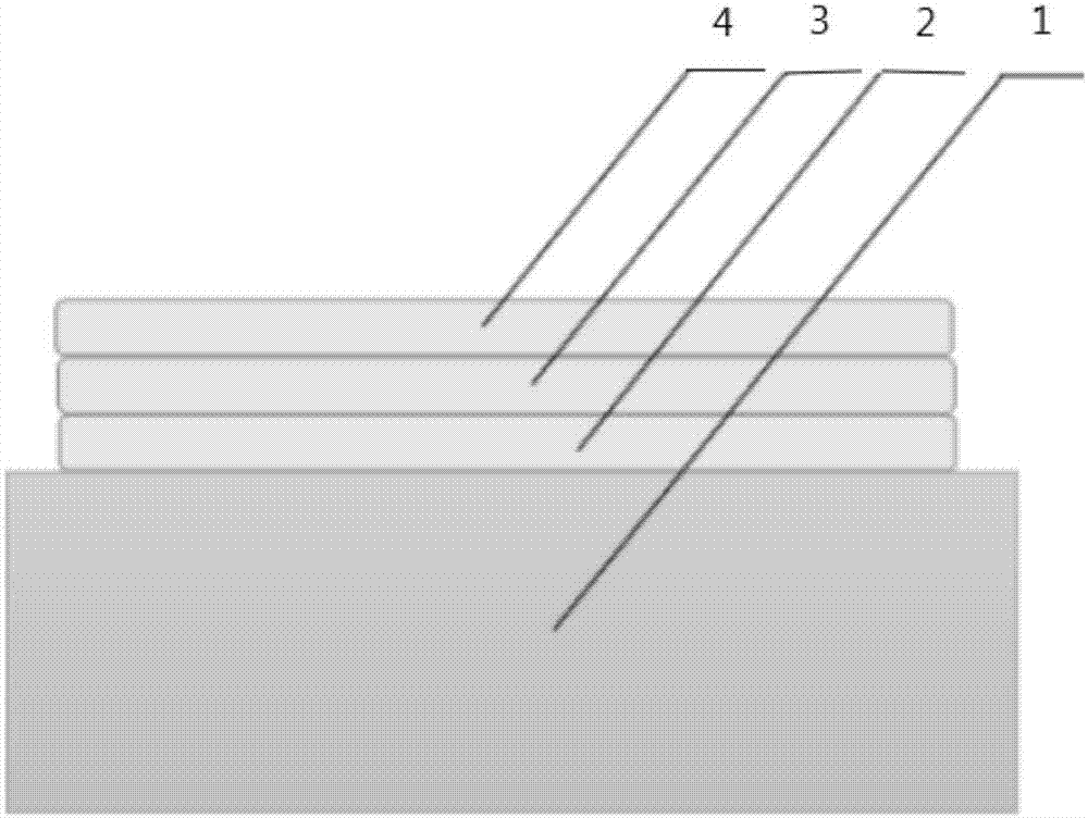
[0050] (1) Provide a germanium doping concentration of 10 19 Atoms / cm 3 Large-scale germanium-doped silicon carbide wafers, prepared by electron beam evaporation 1 × 1mm 2 Titanium-platinum electrodes, in which the thicknesses of Ti, Pt, and Au metal layers are 70nm, 60nm, and 650nm, respectively. A germanium-doped silicon carbide electrode sample was obtained. The schematic diagram of the electrode structure is as figure 1 shown.

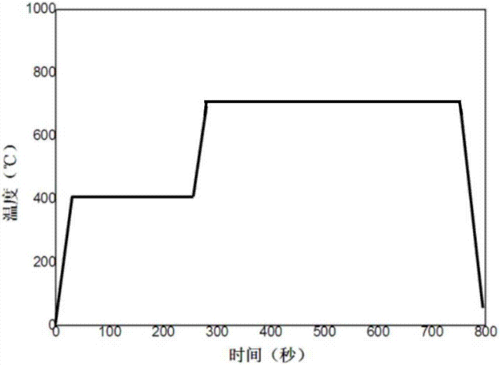
[0051] (2) In the heating stage, the sample is placed in a rapid annealing furnace (RTP) for rapid thermal annealing. The rapid heating stage is divided into two stages. The first stage: the temperature is raised to 400 °C at a heating rate of 16 °C / s. ℃, keep warm for 4 minutes. The second stage: the temperature is raised to 700° C. at a heating rate of 8° C. / second, and the temperature is maintained for 7.5 minutes. The heating surface ...


PUM

PropertyMeasurementUnit
thicknessaaaaaaaaaa
thicknessaaaaaaaaaa
thicknessaaaaaaaaaa

Abstract

The invention relates to a formation method for germanium-doped SiC ohmic contact. The method comprises the steps of forming a Ti/Pt/Au metal electrode on a germanium-doped SiC wafer by electron beam evaporation; performing rapid annealing on the germanium-doped SiC wafer after the electrode is formed to form ohmic contact, wherein rapid annealing is divided into two temperature-rising steps, the temperature of the first stage is risen to 300-500 DEG C and heat preservation is performed for 3-5 mixtures, and the temperature of the second stage is risen to 600-800 DEG C and heat preservation is performed for 5-10 mixtures; and finally, reducing the temperature to a range not higher than 60 DEG C. By doping germanium element, ohmic contact with high quality and low contact resistance is formed; and meanwhile, by changing the concentration of the doped germanium element, germanium-doped SiC products with different ohmic contact properties can be prepared.

Description

technical field [0001] The invention relates to a method for forming an ohmic contact of germanium-doped silicon carbide, which belongs to the field of semiconductor device preparation. Background technique [0002] Silicon carbide (SiC) semiconductor material is the third-generation semiconductor material developed from the first-generation element semiconductor material silicon (Si) and the second-generation compound semiconductor materials gallium arsenide, gallium phosphide, and indium phosphide (GaAs, GaP, InP). One of the new generation wide bandgap semiconductor materials. The third-generation wide bandgap semiconductor materials mainly include silicon carbide (SiC), cubic boron nitride (C-BN), gallium nitride (GaN), aluminum nitride (AlN), zinc selenide (ZnSe) and diamond thin films, etc. [0003] With the in-depth research on silicon carbide crystal materials, we found that silicon carbide crystal materials can be affected differently by doping different elements. ...

Claims


Application Information

Patent Timeline
Patent Type & Authority Applications(China)
IPC IPC(8): H01L21/28H01L21/285
CPCH01L21/0485
Inventor 陈秀芳李天徐现刚胡小波蒋哲
Owner SHANDONG UNIV
Why Eureka
Try Eureka