Method for preparing backside-polished PERC battery

A backside polishing and battery technology, which is applied in the field of backside polishing PERC battery preparation, can solve problems such as unreachable reflectivity, pollution, and increased input costs, and achieve obvious electrical performance gains, elimination of micro-nano structures, and obvious efficiency gains. Effect

Inactive Publication Date: 2017-09-01
HUNAN RED SUN PHOTOELECTRICITY SCI & TECH
View PDF5 Cites 13 Cited by
  • Summary
  • Abstract
  • Description
  • Claims
  • Application Information

AI Technical Summary

Problems solved by technology

In addition to the need to purchase new equipment for this method, some research literature points out that due to the use of alkaline solution in the polishing stage, the metal ions in the solution will contaminate the back surface, and the prepared PERC battery has the problems of low minority carrier lifetime and low efficiency.
[0004] To sum up, the disadvantages of the existing single-side polishing technology for crystalline silicon solar cells mainly lie in: 1. No matter what kind of existing single-side polishing technology, it is necessary to introduce new equipment on the conventional production line, for example, it is necessary to add new Wet chain-type and trough-type equipment, or large-scale transformation of existing equipment, the secondary cleaning equipment of conventional processes loses its use value, and the investment cost of equipment for upgrading conventional battery production lines to PERC battery production lines increases
The introduction of new process technology requires investment in equipment and process debugging, which is also a challenge to conventional production lines
2. In order to balance the subsequent process, the reflectivity cannot reach the designed ideal value; 3. The polishing effect is based on a macroscopic size, that is, the polishing effect is considered to be achieved by characterizing the reflectivity to reach a certain value, but even if it reaches For a certain reflectance value, different polishing methods have great differences in the roughness of the micro-nano structure scale, which will also affect the photoelectric characteristics of crystalline silicon solar cells.
The above-mentioned chemical polishing effects cannot guarantee the flatness on the micro-nano scale. If the method is not proper, it is easy to introduce some micro-nano structures. These micro-nano structures cannot be passivated well during the passivation process, and it is easy to form carrier trapping centers. , greatly reduces the electrical performance of crystalline silicon cells, which is why many manufacturers encounter a large difference between the minority carrier life and the conversion efficiency of the cells although the reflectance is basically the same.
However, based on the characteristics of photovoltaic production control costs and capacity requirements, it is impossible to introduce chemical mechanical polishing (CMP) methods in the field of integrated circuits to achieve micro-nano-scale flatness

Method used


Image

  • Method for preparing backside-polished PERC battery
  • Method for preparing backside-polished PERC battery
  • Method for preparing backside-polished PERC battery

Examples


Embodiment 1

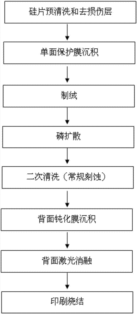
[0036] A preparation method of a backside polished PERC battery of the present invention, such as figure 1 shown, including the following steps:

[0037] (1) Carry out pre-cleaning and dedamage layer to silicon chip, silicon chip is diamond wire cut monocrystalline silicon chip (also can adopt diamond wire cut polysilicon silicon chip), pre-cleaning solution is potassium hydroxide and H 2 o 2 The mixed aqueous solution, the concentration of potassium hydroxide in the solution is 2wt%, and the H in the solution 2 o 2 The concentration is 1wt%, and the treatment time for removing the damaged layer is 5mins. After the treatment, the resulting silicon wafers were washed with deionized water and dried.

[0038] (2) deposit silicon nitride thin film on the silicon wafer back side that step (1) obtains as protective film, the thickness of silicon nitride thin film is 40nm, adopts plasma chemical vapor deposition method (PECVD method) to carry out backside deposition, the process ...

Embodiment 2

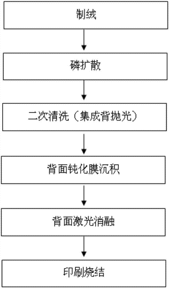
[0044] A preparation method of a backside polished PERC cell of the present invention, comprising the following steps:

[0045] (1) Deposit a silicon oxide film on the back of the silicon wafer as a protective film. The silicon wafer is a diamond wire cut single crystal silicon wafer (diamond wire cut polysilicon silicon wafers can also be used), the thickness of silicon oxide is 20nm, and the silicon oxide film deposition equipment is plasma chemistry. Vapor deposition equipment, the process parameters of the PECVD method used are deposition pressure of 0.15mbar, deposition temperature of 400°C, microwave power of 3000W, silane gas flow of 190sccm, ammonia gas flow of 570sccm, and deposition time of 5mins to obtain a single-sided protective film of silicon wafers.

[0046] (2) the silicon wafer coated with the single-sided protective film obtained in step (1) is carried out using a texture-making process, and the texture-making solution is potassium hydroxide aqueous solution...


PUM

PropertyMeasurementUnit
thicknessaaaaaaaaaa

Abstract

The invention discloses a method for preparing a backside-polished PERC battery. The method comprises: (1), depositing a single-sided protective film on the backside of a silicon wafer; (2) carrying out texturing on the silicon wafer plated with the single-sided protective film and removing the single-sided protective film of the silicon wafer during a pickling process after texturing; (3), carrying out diffusion on the single-sided-textured silicon wafer; (4), carrying out conventional secondary cleaning; and (5), depositing aluminium oxide/silicon nitride laminated passivation film at the back side, carrying out laser grooving, screen printing and sintering, thereby obtaining a backside-polished PERC battery. According to the method disclosed by the invention, the volume production threshold is low; the operation cost is low; micro-nano flatness is realized; and the photoelectric conversion of the battery is improved.

Description

technical field [0001] The invention belongs to the field of crystalline silicon solar cells, and in particular relates to a method for preparing a back-polished PERC cell. Background technique [0002] The effective minority carrier lifetime of crystalline silicon solar cells depends on the recombination rate of the front surface, back surface and matrix. At present, the reduction of the recombination rate of the front surface of industrial crystalline silicon cells is achieved by depositing a silicon nitride anti-reflection film on the front, but there is no special passivation structure to reduce the recombination rate of the back surface. With the advancement of crystalline silicon solar cell technology, the quality of crystalline silicon bulk materials continues to improve, and the back surface recombination of crystalline silicon solar cells has become a bottleneck for further improvement in the efficiency of crystalline silicon solar cells. In order to solve this pro...

Claims


Application Information

Patent Timeline
Patent Type & Authority Applications(China)
IPC IPC(8): H01L31/18H01L31/068
CPCH01L31/068H01L31/1804Y02E10/547Y02P70/50
Inventor 赵保星赵增超周子游刘文峰
Owner HUNAN RED SUN PHOTOELECTRICITY SCI & TECH
Why Eureka
Try Eureka