

Self-alignment grid-based GaN ultrahigh-frequency device and fabrication method thereof
A self-alignment, ultra-high-frequency technology, applied in the field of microelectronics, can solve the problem of weakened gate control capability and device withstand voltage capability, etching accuracy of sidewall expansion of etched grooves, poor uniformity of on-chip devices, etc. problems, to achieve the effect of suppressing current collapse, ensuring power conversion efficiency, and improving yield
- Summary
- Abstract
- Description
- Claims
- Application Information
AI Technical Summary
Problems solved by technology
Method used
Image

Examples
Embodiment 1
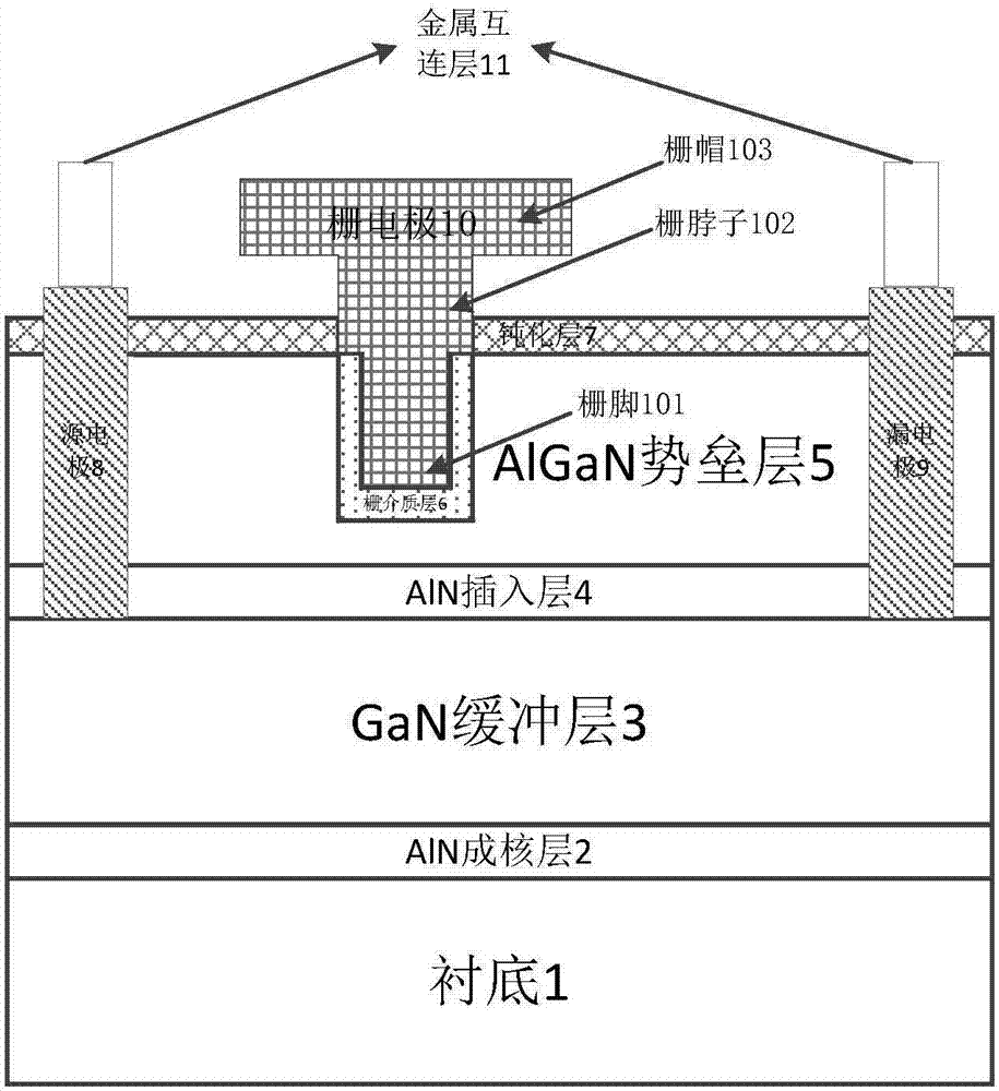
[0035] Embodiment 1: A high-gain ultra-high frequency GaN device structure is fabricated on a SiC substrate with a groove depth of 5 nm, a gate dielectric layer thickness of 4 nm, a passivation layer thickness of 2 nm, and a gate neck height of 160 nm.
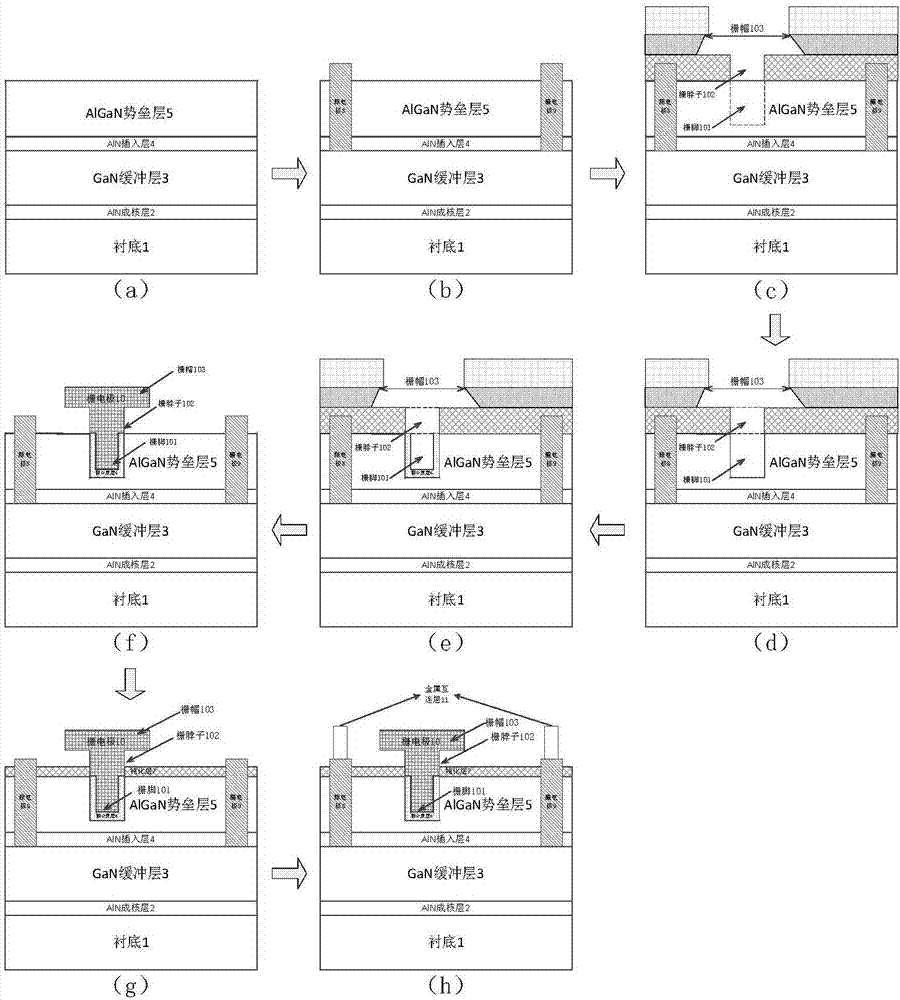
[0036] Step 1, make source electrode 8 and drain electrode 9 on the GaN buffer layer 3 of epitaxial substrate, as figure 2 (b).
[0037] 1a) Photoetching source electrode patterns and drain electrode patterns on the AlGaN barrier layer 5:
[0038] 1a-1) Baking the epitaxial substrate on a hot plate at 200°C for 5 minutes to remove moisture from the substrate;
[0039] 1a-2) On the AlGaN barrier layer 5, apply and spin the peeling glue PMGI-SF6. The thickness of the peeling glue is about 350nm at 2000rpm, and put the formed sample on a hot plate at 200°C. Bake for 5 minutes;
[0040] 1a-3) Carry out the coating and spinning of the photoresist EPI621 on the peeling glue, and the thickness of the peeling glue is 770nm at a sp...
Embodiment 2
[0094] Embodiment 2, a high-gain ultra-high frequency GaN device structure with a groove depth of 12nm, a gate dielectric layer thickness of 4nm, and a passivation layer thickness of 2nm is fabricated on a Si substrate.
[0095] Step 1, make source electrode 8 and drain electrode 9 on the GaN buffer layer 3 of epitaxial substrate, as figure 2 (b).
[0096] 1.1) Source electrode pattern and drain electrode pattern are photolithographically etched on the AlGaN barrier layer 5:
[0097] The concrete realization of this step is identical with the step 1a) among the embodiment one;
[0098] 1.2) Use electron beam evaporation to evaporate the metal on the photolithography area of the electrode to make the electrode:
[0099] The concrete realization of this step is identical with the step 1b) among the embodiment one;
[0100] 1.3) Perform rapid thermal annealing on the sample:
[0101] Put the ohmic metal evaporated and stripped sample into the rapid thermal annealing furnac...
Embodiment 3
[0134] Embodiment 3, a high-gain ultra-high frequency GaN device structure is fabricated on a sapphire substrate with a groove depth of 12 nm, a gate dielectric layer thickness of 8 nm, and a passivation layer thickness of 6 nm.
[0135] Step A, make source electrode 8 and drain electrode 9 on the GaN buffer layer 3 of epitaxial substrate, as figure 2 (b).
[0136] A-1) Source electrode pattern and drain electrode pattern are photolithographically etched on the AGaN barrier layer 5:
[0137] The concrete realization of this step is identical with the step 1a) among the embodiment one;
[0138] A-2) On the AlGaN barrier layer 5 in the source electrode region and the drain electrode region and in the source electrode region and the drain electrode region
[0139] Evaporate source electrode 8 and drain electrode 9 on the outer photoresist:
[0140] The concrete realization of this step is identical with the step 1b) among the embodiment one;
[0141] A-3) Carry out rapid therm...
PUM
| Property | Measurement | Unit |
|---|---|---|
| Thickness | aaaaa | aaaaa |
| Thickness | aaaaa | aaaaa |
| Thickness | aaaaa | aaaaa |
Abstract
Description
Claims
Application Information