Indium gallium nitride thin film on flexible transparent polyimide substrate and preparation method of indium gallium nitride thin film

A transparent polyimide and polyimide technology, which is applied in gaseous chemical plating, semiconductor/solid-state device manufacturing, coating, etc., can solve the problems of poor surface crystallization quality of polyimide substrates, etc.

Active Publication Date: 2018-11-16
DALIAN UNIV OF TECH
View PDF5 Cites 2 Cited by
  • Summary
  • Abstract
  • Description
  • Claims
  • Application Information

AI Technical Summary

Problems solved by technology

However, due to the poor surface crystallization quality of polyimide substrates, it is difficult to directly prepare high crystal quality In on polyimide substrates coated with one-dimensional nanoconductive material layers. x Ga 1-x N film

Method used


Image

  • Indium gallium nitride thin film on flexible transparent polyimide substrate and preparation method of indium gallium nitride thin film
  • Indium gallium nitride thin film on flexible transparent polyimide substrate and preparation method of indium gallium nitride thin film
  • Indium gallium nitride thin film on flexible transparent polyimide substrate and preparation method of indium gallium nitride thin film

Examples


Embodiment 1

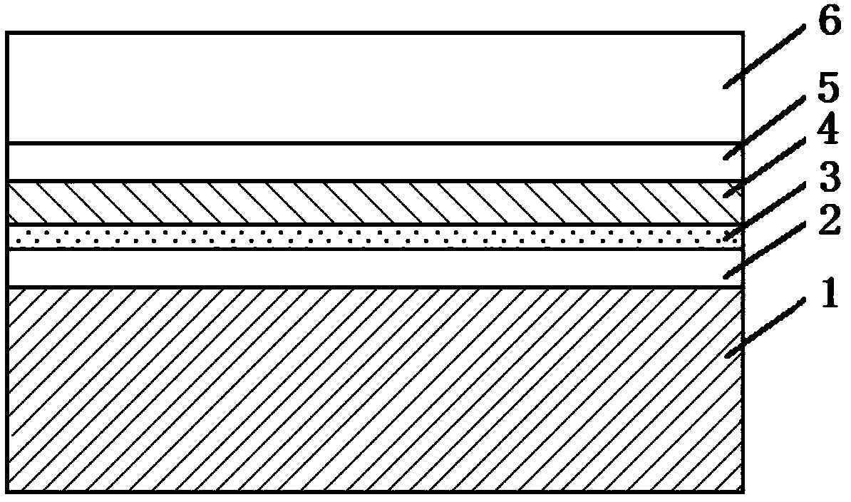
[0030] Embodiment one, such as figure 1 , as shown in 2, 3.

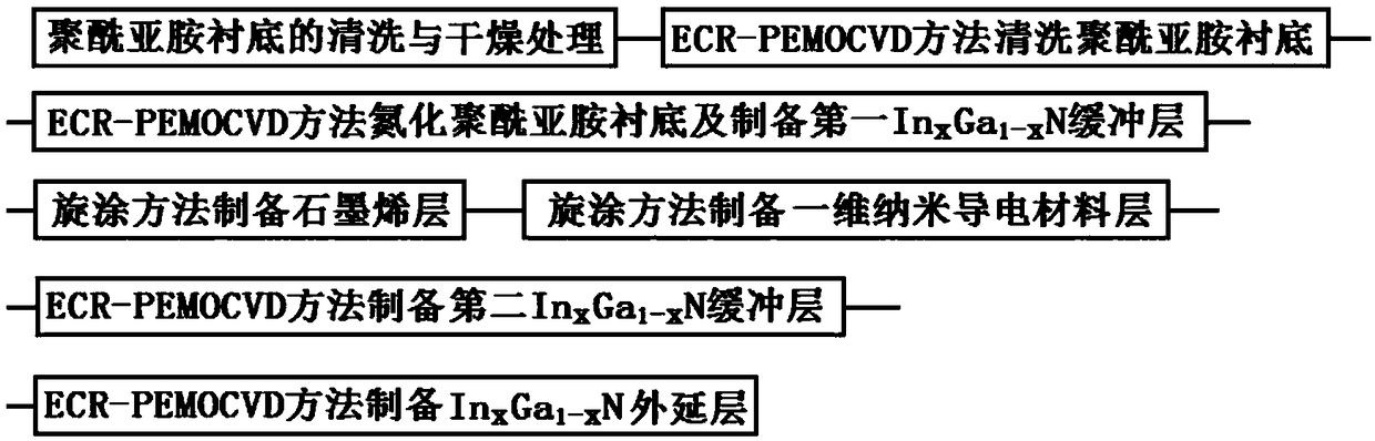
[0031] A kind of using ECR-PEMOCVD equipment (invention patent: ZL201210247144.8), gluing machine and gluing machine, prepared on polyimide substrate 1 as attached figure 1 Shown In 0.55 Ga 0.45 The continuous process steps of N thin film are:

[0032] a. ECR-PEMOCVD method to clean polyimide substrate 1: select a polyimide substrate 1 with a size of 3cm×3cm and a thickness of 200μm, first use a cotton ball soaked in absolute ethanol to wipe the polyimide substrate in one direction The surface of the imide substrate 1 was washed 3 times respectively, and then the polyimide substrate 1 was placed in absolute ethanol and deionized water and ultrasonically cleaned for 3 times, each time for 5 minutes, and then the polyimide substrate 1 was cleaned. Put it on a gluing machine at 120°C for drying treatment for 2 hours, then transfer the polyimide substrate 1 from the glove box of the ECR-PEMOCVD equipment to the samp...

Embodiment 2

[0041] Embodiment two, such as figure 1 , as shown in 2, 3.

[0042] In the second embodiment, except step d, other steps are completely the same as the first embodiment.

[0043] Step d in Example 2. Preparation of carbon nanotube layer 4 by spin coating method: Weigh 10 mg of multi-walled carbon nanotubes and put them into 100 ml of absolute ethanol for 24 hours of ultrasonic vibration to obtain carbon nanotubes with a concentration of 0.1 mg / ml. Nanotube dispersion, the diameter of the carbon nanotubes in the dispersion is 5 to 20nm, and the aspect ratio is 300 to 1200, and the hard substrate adhered to the polyimide substrate 1 is adsorbed on the homogenizer, and then Add the carbon nanotube dispersion liquid onto the graphene layer 3 dropwise, control the speed of the homogenizer to 3500rpm, and prepare the carbon nanotube layer 4 by spin coating, and use a glue baking machine at a temperature of 120°C and a nitrogen atmosphere after spin coating Drying for 5 hours, so ...


PUM

PropertyMeasurementUnit
thicknessaaaaaaaaaa
thicknessaaaaaaaaaa
thicknessaaaaaaaaaa

Abstract

The invention belongs to the technical field of manufacturing of group-III nitride thin films and devices and provides an indium gallium nitride thin film on a flexible transparent polyimide substrateand a preparation method of the indium gallium nitride thin film. Polyimide is taken as a substrate and a first In<x>Ga<1-x>N buffer layer, a graphene layer, a one-dimensional nano-conductive material layer, a second In<x>Ga<1-x>N buffer layer and an In<x>Ga<1-x>N epitaxial layer are sequentially prepared on one side surface of the polyimide substrate from inside to outside, wherein the first In<x>Ga<1-x>N buffer layer, the second In<x>Ga<1-x>N buffer layer and the In<x>Ga<1-x>N epitaxial layer all are prepared by using an electron cyclotron resonance-plasma enhanced metal organic chemical vapor deposition method at low temperature; and the graphene layer and the one-dimensional nano-conductive material layer are prepared by using a spin coating method, so that the prepared high-quality In<x>Ga<1-x>N thin film can be used for preparing flexible transparent devices, such as an indium gallium nitride-based solar cell and a thin-film transistor and has a broad application prospect.

Description

technical field [0001] The invention belongs to the technical field of Group III nitride thin films and device manufacturing, in particular to an indium gallium nitride thin film on a flexible transparent polyimide substrate and a preparation method thereof. On one side of the imine substrate, the first In x Ga 1-x N buffer layer, graphene layer, one-dimensional nano-conductive material layer, second In x Ga 1-x N buffer layer, In x Ga 1-x N epitaxial layer. The first In x Ga 1-x N buffer layer, second In x Ga 1-x N buffer layer and In x Ga 1-x The N epitaxial layer is prepared by electron cyclotron resonance-plasma enhanced metal-organic chemical vapor deposition (ECR-PEMOCVD) method at low temperature, while the graphene layer and the one-dimensional nano conductive material layer are prepared by spin coating method. Background technique [0002] Polyimide (Polymide, PI) has excellent mechanical, insulating, flexible, transparent, radiation resistance, corrosio...

Claims


Application Information

Patent Timeline
Patent Type & Authority Applications(China)
IPC IPC(8): H01L21/02C23C16/44
CPCC23C16/44H01L21/0254H01L21/02587H01L21/0262
Inventor 秦福文马春雨卢康白亦真林国强王德君
Owner DALIAN UNIV OF TECH
Why Eureka
Try Eureka