
An integrated structure of mems piezoelectric printing nozzle assembly

A printing nozzle and piezoelectric technology, applied in printing and other directions, can solve the problems of affecting the life of CMOS circuits, affecting the performance of CMOS circuits, and being uneconomical, and achieve the effects of reducing Joule heat consumption, reducing size, and improving performance.

Active Publication Date: 2019-07-23
珠海天成先进半导体科技有限公司
View PDF7 Cites 0 Cited by
  • Summary
  • Abstract
  • Description
  • Claims
  • Application Information

AI Technical Summary

Problems solved by technology

First prepare a CMOS integrated circuit on an SOI wafer, then dig out the piezoelectric ink cavity and movable diaphragm from the back of the wafer, and prepare ink supply grooves and nozzles on the other wafer using MEMS technology, and use wafer stacking The bonding process aligns and adheres the above two wafers together, and finally forms a piezoelectric material on the top of the active diaphragm area. The disadvantages are as follows: (1) The part of the CMOS integrated circuit located on the active diaphragm is under piezoelectric braking. It also moves together. The stress and strain in the silicon lattice will change the carrier mobility in the semiconductor and affect the performance of this part of the CMOS circuit. At the same time, the long-term periodic deformation will also affect the life of the CMOS circuit.
(2) The CMOS circuits on the wafer are not fully arranged, that is, there is a large amount of free area, which is uneconomical for the CMOS process charged by area
(3) The piezoelectric material is finally formed, and there are strict restrictions on the preparation process of the piezoelectric material, especially the process temperature
Therefore, constructing integrated structures of MEMS piezoelectric inkjet printheads with high nozzle density, low cost, high efficiency and reliability remains an ongoing challenge.

Method used


Image

  • An integrated structure of mems piezoelectric printing nozzle assembly
  • An integrated structure of mems piezoelectric printing nozzle assembly
  • An integrated structure of mems piezoelectric printing nozzle assembly

Examples


Embodiment 1

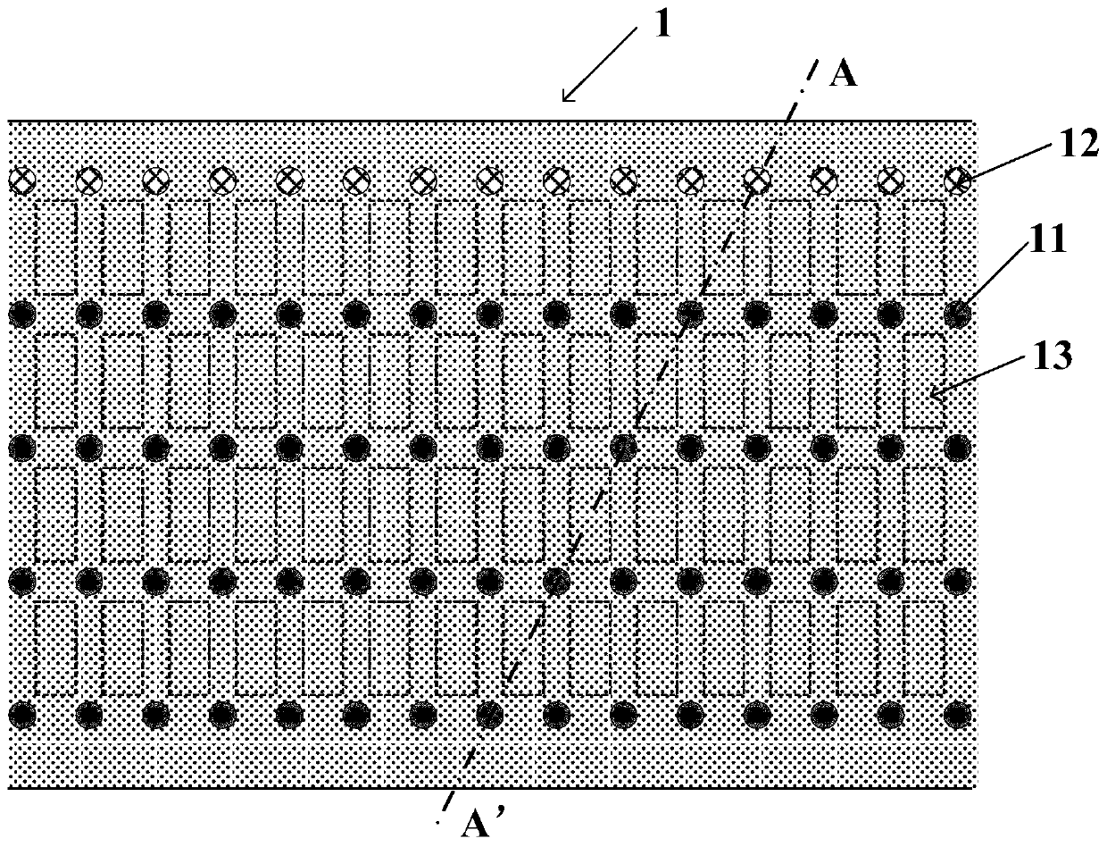
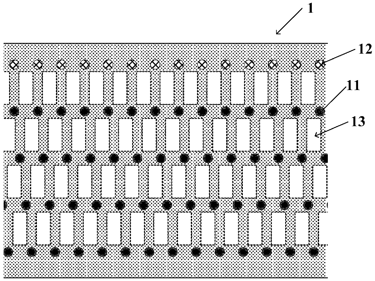
[0068] Nozzle density is an important technical indicator of inkjet print head, the higher the nozzle density, the higher the resolution of the print head. Due to the limitation of the minimum pitch of nozzles, the density of a single row of nozzles is very limited, and the use of multiple rows of nozzles to form a nozzle array is an effective means to increase the density of nozzles. The MEMS piezoelectric print head chip of the nozzle array is narrow and long, with a width of about 1 cm and a length of 7 to 10 cm. Due to the large aspect ratio, only a part of the MEMS piezoelectric print head chip (component) along the length direction is shown in the figure.

[0069] figure 1 An example of a schematic plan view of a nozzle array composed of 4 rows of nozzles is given in , where there is no misalignment among the rows of 4 nozzles. For brevity, figure 1 Only the array arrangement of the corresponding ink chambers 13 is drawn in the figure. Normally, the nozzles 17 are des...

Embodiment 2

[0096] see Figure 15 , Flip-chip the drive / control integrated circuit chip 23 on the package substrate 26, and set the underfill material 25; then through the solder ball 27, realize the electrical connection with the silicon transfer substrate 2, thereby realizing the MEMS piezoelectricity with the nozzle array The electrical connection of the print head chip 1. The silicon transfer substrate 2 and the driving / control integrated circuit chip 23 are flip-chip mounted on the same surface of the package substrate 26 , and the silicon transfer substrate 2 is located above the driving / control integrated circuit chip 23 . The solder balls 27 are distributed around the silicon interposer substrate 2 avoiding the area of ​​the driving / control integrated circuit chip 23 . The height of the solder ball 27 is greater than the sum of the thickness of the driving / control integrated circuit chip 23 and the height of the bump 24 . An underfill material 25 is applied between the driving / c...

Embodiment 3

[0099] The speed of each I / O pin of the driving / control integrated circuit chip 23 is not high, and the wire bonding can also meet the current capacity, DC voltage drop and signal integrity of each I / O pin of the driving / control integrated circuit chip 23 To meet the requirements of safety, wire bonding can be used instead of flip-chip bump bonding in Embodiment 2 to realize the micro-assembly of the driving / control integrated circuit chip 23 on the packaging substrate 26, so as to further reduce the difficulty of micro-assembly. Simultaneously, because the driving / control integrated circuit chip 23 is directly mounted on the packaging substrate 26, the thermal resistance between the driving / control integrated circuit chip 23 and the packaging substrate 26 is smaller than that of embodiment two, so the driving / control integrated circuit chip 23 is dissipated. Effect is better than embodiment two. For the structural schematic diagram of the third embodiment of the MEMS piezoele...


PUM

PropertyMeasurementUnit
Widthaaaaaaaaaa
Lengthaaaaaaaaaa
Diameteraaaaaaaaaa

Abstract

The invention discloses an MEMS piezoelectric printing nozzle assembly integrated structure. An MEMS piezoelectric printing nozzle chip is disposed on one side of a silicon adapter substrate, and a packaging substrate is disposed on the other side of the silicon adapter substrate; a driving / control integrated circuit chip is disposed between the silicon adapter substrate and the packaging substrate; a heat sink is disposed on the other side of the packaging substrate, and one end of the packaging substrate is electrically connected to an electrical interface through a flexible circuit board; the MEMS piezoelectric print nozzle chip is formed by allowing silicon wafer bonding to form ink chambers arranged in an array; a nozzle is correspondingly disposed on the bottom of each ink chamber; and metal wiring layers disposed on the upper and lower surfaces of the silicon adapter substrate are electrically connected to TSV via holes extending through the silicon adapter substrate. The structure reduces the size of the integrated packaging of the print nozzle assembly, ensures the shortest electrical interconnect length and minimum interconnect resistance, reduces the Joule heat consumption of the print nozzle assembly through the small interconnect resistance, and reduces parasitic parameters such as interconnection resistance, capacitance and inductance, reduces signal transmissionloss, delay, and distortion, and can improve the performance of the printing head.

Description

technical field [0001] The invention belongs to the technical field of advanced electronic packaging, and in particular relates to an integrated structure of a MEMS piezoelectric printing nozzle assembly. Background technique [0002] The MEMS piezoelectric inkjet print head has the characteristics of high resolution and high scalability, and is especially suitable for emerging industrial market applications such as printed electronics, packaging, textiles, and 3D printing. Compared with using a whole piece of piezoelectric ceramic body material as a brake, the piezoelectric ceramic thin film deposited by sol-gel method or sputtering method can better control the ink droplet size to adjust the gray value and reduce power consumption, And it has become the mainstream piezoelectric actuator in the MEMS piezoelectric inkjet print head. In order to obtain high-quality printing effects, each nozzle of the print head needs to be electrically driven and controlled independently, t...

Claims


Application Information

Patent Timeline
IPC IPC(8): B41J2/14
CPCB41J2/14201
Inventor 李宝霞
Owner 珠海天成先进半导体科技有限公司
Learn More