


Quick Research
Generate reliable direction feasibility study reports for your R&D in just a few steps.

Technical Q&A
Discover and master advanced knowledge NOW. Basics, ideas, possibilities, all at once.

Find Solutions
As an expert in R&D theories, this can generate solutions to your technical problems instantly.

Evaluate Feasibility
Analyze your overall solution with one click, know your potential R&D risks in advance.

Monitor Landscape
Get weekly tech updates, stay abreast of the latest tech innovations and key insights.
Picoliter-magnitude ultramicro-amount injector based on patterned surface and preparation method thereof
A patterned surface and ultra-micro-volume technology, applied in the field of material science, can solve the problems of complex preparation process, difficulty in micro-fluidic device manipulation, high cost of digital micro-fluidics, etc., to achieve simple preparation process, simplified processing difficulty, and operation simple effect
- Summary
- Abstract
- Description
- Claims
- Application Information
AI Technical Summary
Problems solved by technology
Method used
Image

Examples
Embodiment 1
[0035] Embodiment 1: the preparation of hydrophilic substrate
[0036] The substrate used is a single crystal silicon wafer (100). Cut the substrate to a size of 3cm in length and 2cm in width with a glass knife, and place it in acetone, ethanol and deionized water for three times for ultrasonication, each time for 1-2 minutes, and then put the mass fraction 98% concentrated sulfuric acid and a mass fraction of 30% hydrogen peroxide mixed solution (volume ratio is 7:3) in a water bath heated to 120 ° C, kept for 5 hours to obtain a hydrophilic substrate; then pour the mixed acid solution into the waste In the liquid bottle, the obtained substrate was repeatedly ultrasonically washed 5 times with deionized water, each time for 1-2 minutes, and stored in deionized water for later use.
Embodiment 2
[0037] Example 2: Preparation of patterned photoresist array structure substrate
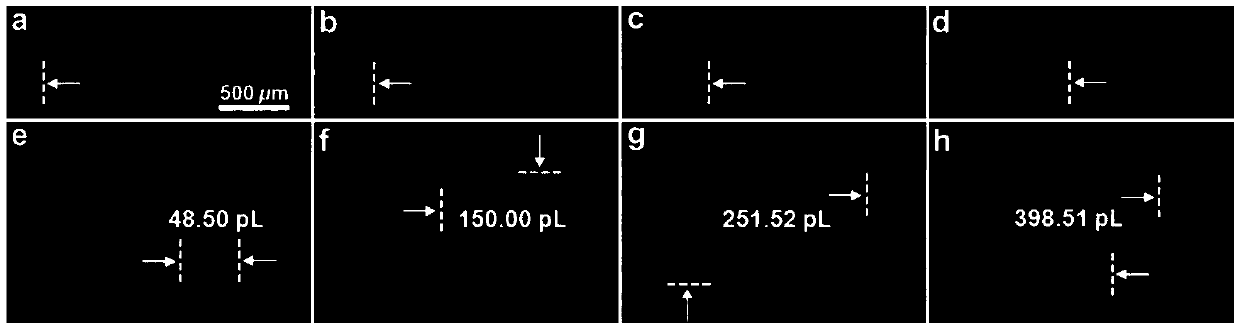
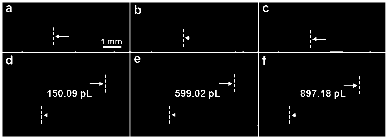
[0038] The silicon wafer was cleaned in an oxygen plasma cleaning machine for 5 minutes, and then a layer of photoresist was spin-coated on the silicon wafer surface (the spin-coating condition was 3000rpm, 60s); UV exposure under the template for 10-30s, UV exposure for 14s, and then immerse the silicon wafer in a special developer solution for 30s to obtain a patterned photoresist surface. According to the required liquid volume and range, we designed a Responsive strip mask, different photolithographic mask patterns, we get a variety of patterned photoresist surfaces with different patterns and matching with a variety of chip microchannels; wherein, the patterned microstructure array mask is Chromium layer patterned and film-printed array of micron-scale stripes.
Embodiment 3
[0039] Example 3: Preparation of Hydrophobic Patterned Silicon Structure Array Structure Substrate
[0040] Place the patterned photoresist array structure substrate obtained in Example 2 in the cavity of a plasma etching machine, and the etching time is 10min (the etching pressure is 6mTorr, the etching temperature is 10°C, the etching power is 50W for RF, and the ICP 100W); then place the substrate in absolute ethanol for ultrasonic cleaning for 10 minutes to remove residual photoresist on the surface, then ultrasonically clean it with deionized water for 5 minutes, and dry it with nitrogen; place the obtained substrate in an oxygen plasma cleaning machine The surface of the substrate was cleaned with hydroxyl groups for 5 minutes, and then the surface of the substrate was grafted with 1H, 1H, 2H, 2H-perfluorooctyltrichlorosilane by vapor deposition to obtain a hydrophobic patterned silicon structure array. Depending on the resist pattern, we can obtain patterned silicon str...
PUM
| Property | Measurement | Unit |
|---|---|---|
| Thickness | aaaaa | aaaaa |
| Etching power | aaaaa | aaaaa |
Abstract
Description
Claims
Application Information
 - R&D Engineer
- R&D Manager
- IP Professional
- Industry Leading Data Capabilities
- Powerful AI technology
- Patent DNA Extraction
Browse by: Latest US Patents, China's latest patents, Technical Efficacy Thesaurus, Application Domain, Technology Topic, Popular Technical Reports.
© 2024 PatSnap. All rights reserved.Legal|Privacy policy|Modern Slavery Act Transparency Statement|Sitemap|About US| Contact US: help@patsnap.com