
Tin dioxide/zinc oxide composite nanowire material and preparation method thereof

A technology of zinc oxide nanowires and tin dioxide, applied in nanotechnology, semiconductor/solid-state device manufacturing, organic semiconductor devices, etc., can solve the problem of increased electron and hole recombination probability, increased electron transmission path, and reduced solar cell efficiency etc. to achieve the effects of increasing light absorption, reducing transmission paths, and improving photoelectric conversion efficiency

Pending Publication Date: 2019-08-06
NANJING UNIV OF POSTS & TELECOMM
View PDF1 Cites 4 Cited by
  • Summary
  • Abstract
  • Description
  • Claims
  • Application Information

AI Technical Summary

Problems solved by technology

However, the growth crystal planes and growth directions of tin dioxide nanowires prepared by chemical vapor deposition are different. This disorder increases the path of electron transport, and the recombination probability of electrons and holes is greatly increased. The efficiency of the entire solar cell will also decrease accordingly

Method used


Image

  • Tin dioxide/zinc oxide composite nanowire material and preparation method thereof
  • Tin dioxide/zinc oxide composite nanowire material and preparation method thereof
  • Tin dioxide/zinc oxide composite nanowire material and preparation method thereof

Examples


Embodiment 1

[0024] The tin dioxide / zinc oxide composite nanowire material in this embodiment includes a tin dioxide nanowire array substrate and a zinc oxide nanowire array grown on the substrate. Wherein, the length of the tin dioxide nanowire is 300nm and the diameter is 50nm, and the length of the zinc oxide nanowire is 500nm.

[0025] The preparation method of the composite nanowire material comprises the following steps:

[0026] (1) Preparation of anodized aluminum nanoporous template: wash the 1.5×1.5 cm FTO conductive substrate with toluene, acetone, ethanol and deionized water respectively. Using thermal evaporation method to A thermal evaporation rate of 300 nm of aluminum was deposited on the FTO conductive substrate, and the sample holder was rotated during the deposition to ensure uniform film thickness. Then use a copper strip to contact the surface of the aluminum, seal the substrate in the electrolytic cell, use the method of anodic oxidation, use a platinum mesh electr...

Embodiment 2

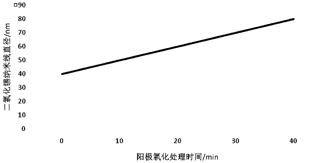
[0034] Design 5 groups of comparative tests, test procedure is basically the same as embodiment 1, difference is the anodic oxidation time in step (1), concrete time is shown in Table 1, then the tin dioxide nanowire material diameter of preparation is compared, The results obtained are shown in Table 1 below.

[0035] Tin dioxide nanowire diameter comparison table prepared by different anodizing time in table 1

[0036]

[0037] It can be seen from Table 1 that with the increase of anodization time, the diameter of tin dioxide nanowires gradually increases. If the tin dioxide nanowire diameter is too large, it is not conducive to perovskite penetration in the tin dioxide nanowire, if the diameter of the tin dioxide nanowire is too small, when the zinc oxide nanowire seed layer is spin-coated, the seed layer solution will penetrate Into the gap of the nanowires, so that the zinc oxide nanowires cannot grow on the tin dioxide nanowires, so we choose the anodizing time as 10...

Embodiment 3

[0039] The tin dioxide / zinc oxide composite nanowire material of the present invention comprises a tin dioxide nanowire array substrate and a zinc oxide nanowire array grown on the substrate. Wherein, the length of the tin dioxide nanowire is 400nm and the diameter is 60nm, and the length of the zinc oxide nanowire is 500nm.

[0040] The preparation method of the composite nanowire material comprises the following steps:

[0041] (1) Preparation of anodized aluminum nanoporous template: wash the 1.5×1.5 cm FTO conductive substrate with toluene, acetone, ethanol and deionized water respectively. Using thermal evaporation method to A thermal evaporation rate of 400 nm of aluminum was deposited on the FTO conductive substrate, and the sample holder was rotated during the deposition to ensure uniform film thickness. Then use a copper strip to contact the surface of the aluminum, seal the substrate in the electrolytic cell, and use an anodic oxidation method to use a platinum me...


PUM

PropertyMeasurementUnit
Lengthaaaaaaaaaa
Lengthaaaaaaaaaa
Lengthaaaaaaaaaa

Abstract

The invention discloses a tin dioxide / zinc oxide composite nanowire material and a preparation method thereof. The material comprises a tin dioxide nanowire array made of anodic alumina nanopores as atemplate and zinc oxide nanowires grown thereon. Aluminum is deposited on an FTO conductive substrate, the formation of nanopores is induced by anodic oxidation in an acidic electrolyte environment,diluted tin dioxide colloid solution and zinc oxide nanowire seed layer solution are applied by spin-coating, and finally, the treated FTO conductive substrate is put in the aqueous solution of zinc acetate dihydrate and hexamethylenetetramine to grow zinc oxide nanowires. The product of the invention is highly vertically ordered. The transmission path of charges in the electron transport layer isgreatly reduced, the transmission and separation of electron-hole pairs are facilitated, and the scattering of photons and the absorption of light are increased. Because of the adjustment of the energy level of conduction band between perovskite and the electron transport layer, the electron transport barrier is reduced, the efficiency of electron extraction is improved, and the probability of electron-hole recombination is reduced.

Description

technical field [0001] The invention relates to a nanocomposite material and a preparation method, in particular to a tin dioxide / zinc oxide composite nanowire material and a preparation method thereof. Background technique [0002] Tin dioxide nanowires are generally prepared by chemical vapor deposition. The main step is to mix tin powder and stannous oxide powder evenly, form tin dioxide by chemical reaction at high temperature and mix it with carrier gas, and evenly send it to the reaction chamber. SnO nanowires were fabricated on high-temperature substrates. However, the growth crystal planes and growth directions of the tin dioxide nanowires prepared by chemical vapor deposition are different. This disorder increases the path of electron transport, and the recombination probability of electrons and holes is greatly increased. The efficiency of the entire solar cell will also decrease accordingly. The tin dioxide nanowires are perpendicular to the FTO conductive subst...

Claims


Application Information

Patent Timeline
IPC IPC(8): H01L51/46H01L51/42H01L51/44H01L51/48B82Y40/00
CPCB82Y40/00H10K71/00H10K30/352H10K30/87H10K2102/00Y02E10/549
Inventor 鞠维刘利清张红光
Owner NANJING UNIV OF POSTS & TELECOMM
Learn More